Method for forming a tantalum oxide capacitor using two-step rapid thermal nitridation

a technology of tantalum oxide dielectric and thermal nitridation, which is applied in the direction of capacitors, semiconductor devices, electrical apparatus, etc., can solve the problems of reducing the refresh time, reducing the reliability and yield ratio of the capacitor, and reducing the size of the memory cell

Inactive Publication Date: 2001-03-27
SAMSUNG ELECTRONICS CO LTD
View PDF7 Cites 27 Cited by
  • Summary
  • Abstract
  • Description
  • Claims
  • Application Information

AI Technical Summary

Problems solved by technology

However, as semiconductor devices becomes more highly integrated and device geometries become finer, each memory cell becomes smaller and lower operational voltages are used.
If the capacitance is insufficient, the refresh time is reduced, and the reliability and yield ratio thereof deteriorate.
However, even though increased integration levels result in increased leakage current, acceptable devices are still obtained, and production efficiency increases, if the capacitance exceeds a predetermined level.
s greater. That is, when the RTN process is performed at 900.degree. C., the characteristics of the lower structure such as the storage electrode are de
When the RTN is performed at 850.degree. C., the agglomeration of HSGs is suppressed, however, a thickness of the nitride layer produced therefrom is limited to a predetermined level.
When the RTN-process is perf...

Method used


Image

  • Method for forming a tantalum oxide capacitor using two-step rapid thermal nitridation
  • Method for forming a tantalum oxide capacitor using two-step rapid thermal nitridation
  • Method for forming a tantalum oxide capacitor using two-step rapid thermal nitridation

Examples


Embodiment Construction

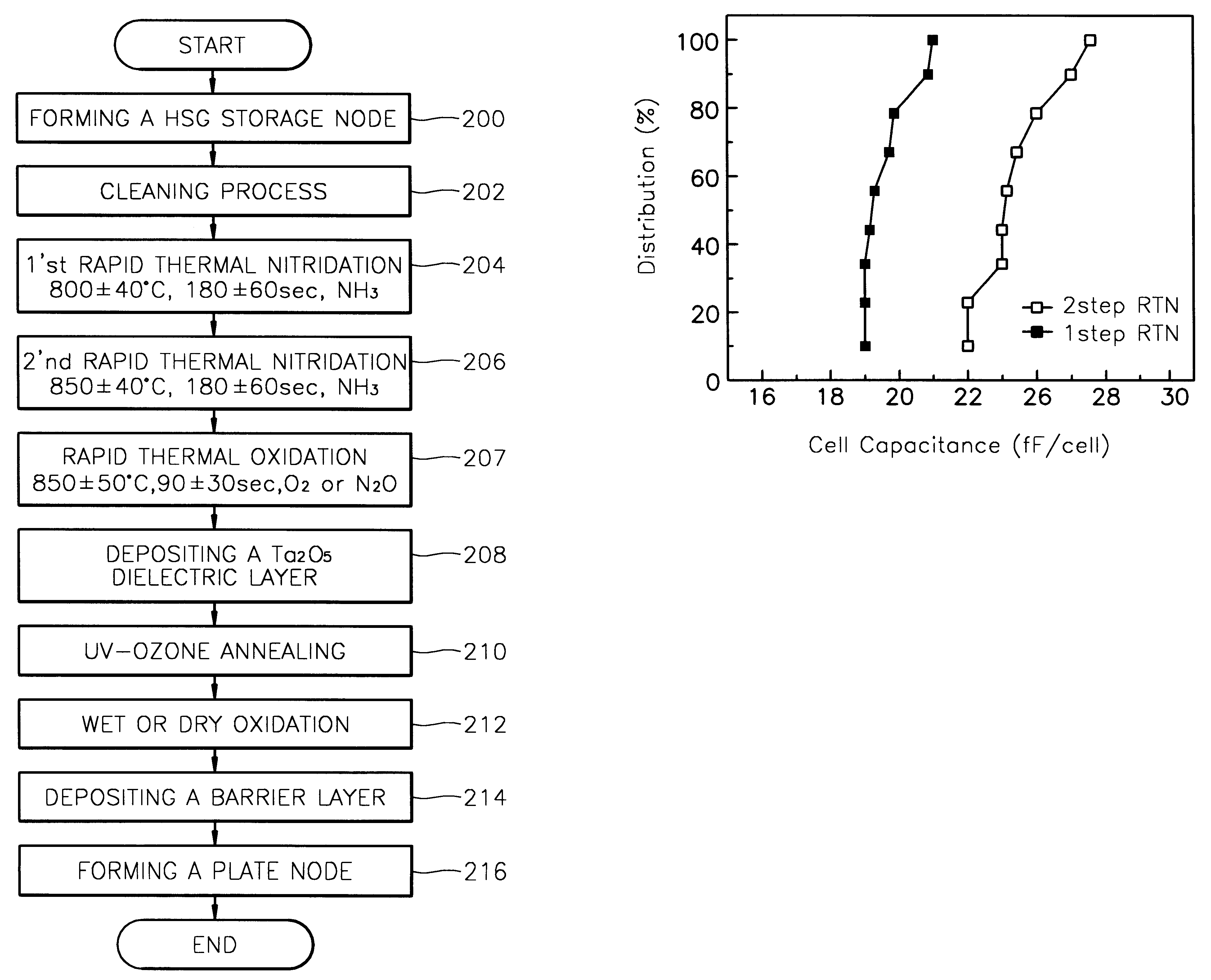
FIG. 6 is a graph illustrating the difference in cell capacitance between an exemplary device formed through the conventional one step RTN process at 900.degree. C. and an exemplary device formed through a two step RTN process according to the present invention at 800.degree. C. and 850.degree. C. Referring to FIG. 6, the Y-axis indicates a distribution (%) of measured points and the X-axis indicates cell capacitance values (fF / cell). When the one step RTN is performed at 900.degree. C., i.e., in a line represented by (.box-solid.), the capacitance of the resulting cells is 19.about.21.2 fF / cell. This is because HSGs on the surface of a storage node are agglomerated due to the high temperature of 900.degree. C., thereby reducing the overall surface area of the storage node. However, with the two step RTN performed at 800.degree. C. and 850.degree. C., i.e., in a line represented by (.quadrature.), the capacitance of the resultant cells is 22.about.25.5 fF / cell. This is because a rel...


PUM


Abstract

A method for forming a Ta2O5 capacitor on a semiconductor device reduces leakage current and increases cell capacitance by utilizing a two-step rapid thermal nitridation (RTN) process to form a nitride layer on a hemi-spherical grain (HSG) storage node. The first RTN process is performed in a NH3 atmosphere at 800±40° C. for 180±60 seconds, thereby forming a nitride layer having a thickness of about 4 Å. The second RTN process is performed in a NH3 atmosphere at 850±40° C. for 180±60 seconds, thereby increasing the thickness of the nitride layer to at least about 7 Å. Therefore, a nitride layer that is thick enough to act as an oxidation barrier is achieved, but agglomeration of the HSGs on the storage node due to high process temperatures is prevented. To make the structure more readily adaptable to process for manufacturing DRAMs with Ta2O5 dielectric layers, a rapid thermal oxidation (RTO) process can then be performed in an O2 or N2O atmosphere at 850±50° C. for 90±30 seconds to thereby form a combined layer comprising a nitride layer and an oxide layer.

Description

This application corresponds to Korean patent application No. 97-54217 filed Oct. 22, 1997 in the name of Samsung Electronics Co., Ltd., which is herein incorporated by reference for all purposes.1. Field of the InventionThis invention relates generally to capacitors for semiconductor devices, and more particularly, to a method for forming a capacitor having a tantalum oxide dielectric using a two-step rapid thermal nitridation process.2. Description of the Related ArtIn general, each memory cell of a dynamic random access memory (DRAM) includes one capacitor and one transistor. Each capacitor, which is used for storing information, is very important for the DRAM device. However, as semiconductor devices becomes more highly integrated and device geometries become finer, each memory cell becomes smaller and lower operational voltages are used. Accordingly, it is necessary to increase the capacitance of each capacitor to obtain the desired drive characteristics for each cell. If the c...

Claims


Application Information

Patent Timeline
IPC IPC(8): H01L21/02H01L21/321H01L21/316H01L21/70H01L21/8242H01L21/8247H01L27/04H01L27/108H01L27/115H01L29/788H01L29/792
CPCH01L21/3211H01L21/31604H01L27/1085H01L28/56Y10S438/964H01L21/02255H01L21/02326H01L21/02271H01L21/02247H01L21/02183H10B12/03H01L27/04H10B12/00H01L21/02348
Inventor HWANG, KI-HYUNPARK, JAE-YOUNGBYUN, JAE-HO
Owner SAMSUNG ELECTRONICS CO LTD
Why Eureka
Try Eureka