Optimized decoupling capacitor using lithographic dummy filler

Inactive Publication Date: 2001-05-15
SAMSUNG ELECTRONICS CO LTD +1
View PDF2 Cites 22 Cited by
  • Summary
  • Abstract
  • Description
  • Claims
  • Application Information

AI Technical Summary

Problems solved by technology

Whether externally provided or internally generated, power supply voltage levels on advanced DRAM arrays, may typically vary from -0.5V to about 3.5V, which makes it difficult to implement sufficient decoupling capacitors for all types of power supplies.
Moreover, such capacitors require a large amount of chip area which makes it difficult to find space on the chip to provide enough decoupling capacitors for each power supply.
For large arrays, the area wasted by dummy patterns can be significant.

Method used


Image

  • Optimized decoupling capacitor using lithographic dummy filler
  • Optimized decoupling capacitor using lithographic dummy filler
  • Optimized decoupling capacitor using lithographic dummy filler

Examples


Embodiment Construction

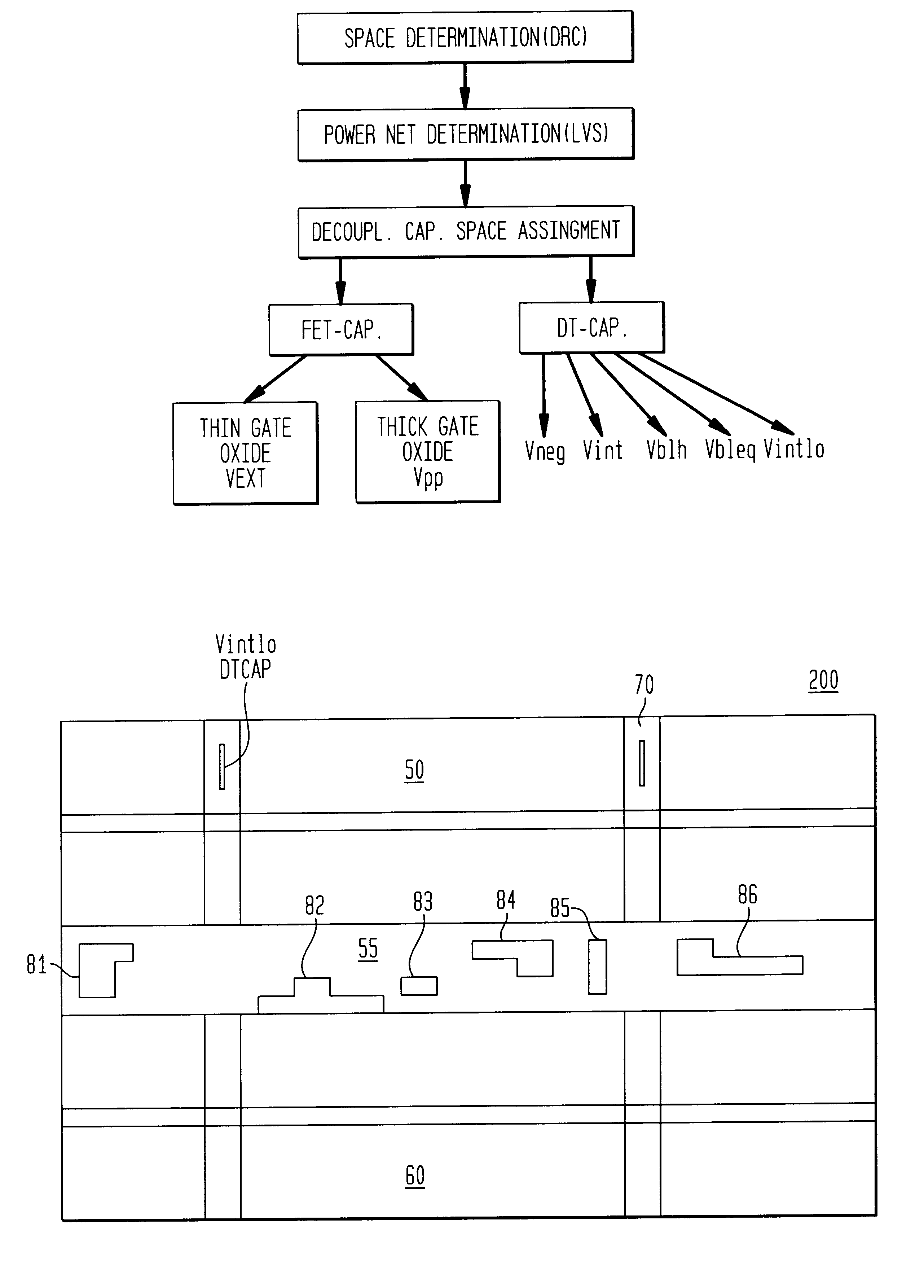
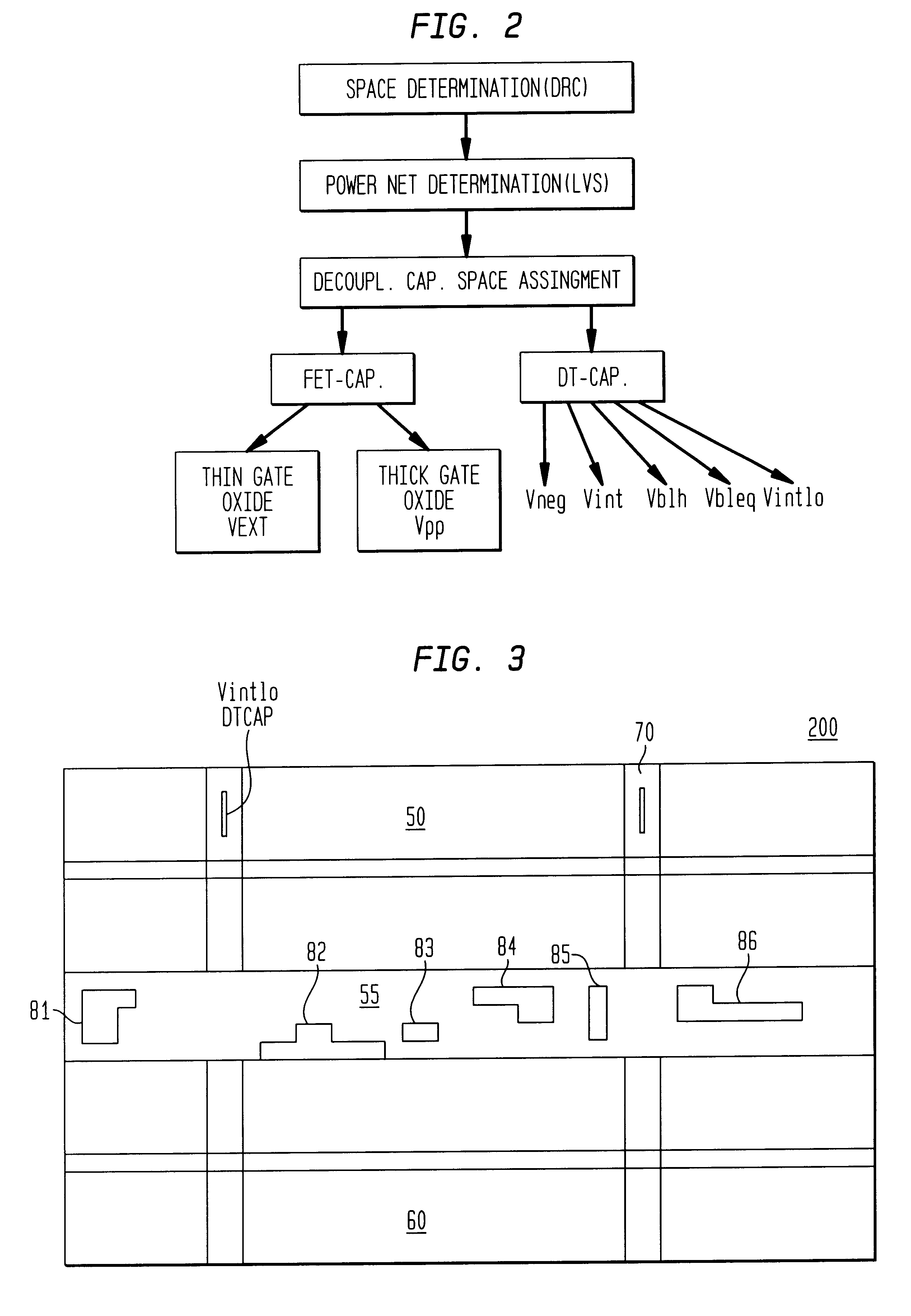
As mentioned above, it is common to form dummy patterns around the edge of a semiconductor chip array to avoid problems associated with the non-uniform patterns which form along the edges of an array. Conventional structures leave the dummy patterns unused. The preferred embodiments of the present invention take advantage of these unused portions of the chip by creating passive devices such as decoupling capacitors in the unused dummy patterns.

Before discussing preferred embodiments in detail, a general discussion of the usefulness of dummy filler lithography with respect to a DRAM chip will be presented.

In high density DRAM designs, a boosted wordline voltage is usually generated internally by a charge pump and regulated by a voltage regulator. A reservoir capacitor keeps the boosted level voltage relatively stable. During DRAM operations, such as reading or writing to or from a cell, the wordlines are accessed with a boosted voltage (Vpp). This voltage is normally much higher than...


PUM


Abstract

A method to optimize the size and filling of decoupling capacitors for very large scale integrated circuits (VLSI) using existing lithographic fillers. The method combines the automatic or manual generation of lithographic fill patterns with the forming of the capacitors. According to the method, when the chip layout is about to be finished, all remaining empty space on the chip gets identified by a layout tool. Then, the closest power-supply nets get extracted. All power supplies and their combinations are sorted in a connection table which determines the appropriate types of capacitances once the power-supply nets closest to the empty spaces extracted from the layout. The empty spaces are then assigned appropriate decoupling capacitances. Decoupling capacitors generated by the method are suitable for VLSI power supplies for noise reduction.

Description

1. Field of the InventionThe present invention generally relates to the formation of capacitors in semiconductor circuits, and more specifically to the utilization of unused "dummy" border areas of the DRAM arrays as decoupling capacitors and other useful structures in logic and memory arrays.2. Description of the Related ArtIn order to minimize noise effects, decoupling capacitors are often needed in very large scale integration (VLSI) circuits, to be attached in the various type of power supplies of logic and memory array circuits. Whether externally provided or internally generated, power supply voltage levels on advanced DRAM arrays, may typically vary from -0.5V to about 3.5V, which makes it difficult to implement sufficient decoupling capacitors for all types of power supplies. For example, voltages such as the boosted wordline voltage, are too high to be applied on a deep trench decoupling capacitor where reliability of the dielectric is a key concern. Moreover, such capacito...

Claims


Application Information

Patent Timeline
IPC IPC(8): H01L21/02H01L21/70H01L21/8242H01L27/108G06F17/50H01L21/82H01L21/822H01L27/04
CPCH01L28/40H01L27/10861H01L27/10894H01L27/10897H10B12/038H10B12/09H10B12/50H10B12/00
Inventor REITH, ARMIN M.HSU, LOUISHAFFNER, HENNINGLEHMANN, GUNTHER
Owner SAMSUNG ELECTRONICS CO LTD
Why Eureka
Try Eureka