Semiconductor structure having reduced silicide resistance between closely spaced gates and method of fabrication

Inactive Publication Date: 2001-05-22
IBM CORP
View PDF11 Cites 116 Cited by
  • Summary
  • Abstract
  • Description
  • Claims
  • Application Information

AI Technical Summary

Benefits of technology

The present invention provides for increasing the space available for silicide formation between closely spaced gate structures thereby lowering the diffusion resistance. In particular, the present invention provides for an effectively narrower spacer between gate structures during silicide formation without degrading the device short channel behavior. More particularly, the present invention provides for a p

Problems solved by technology

However, as device dimensions shrink, so does the spacing between adjacent gate structures.
The formation of silicide in

Method used


Image

  • Semiconductor structure having reduced silicide resistance between closely spaced gates and method of fabrication
  • Semiconductor structure having reduced silicide resistance between closely spaced gates and method of fabrication
  • Semiconductor structure having reduced silicide resistance between closely spaced gates and method of fabrication

Examples


Example

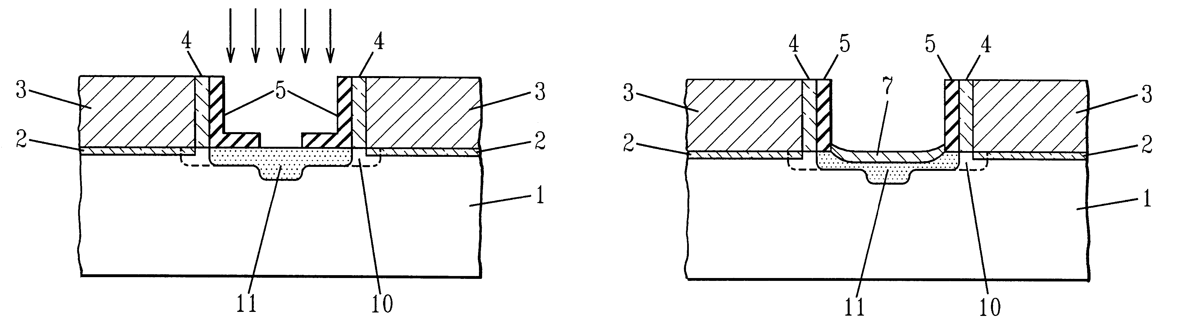
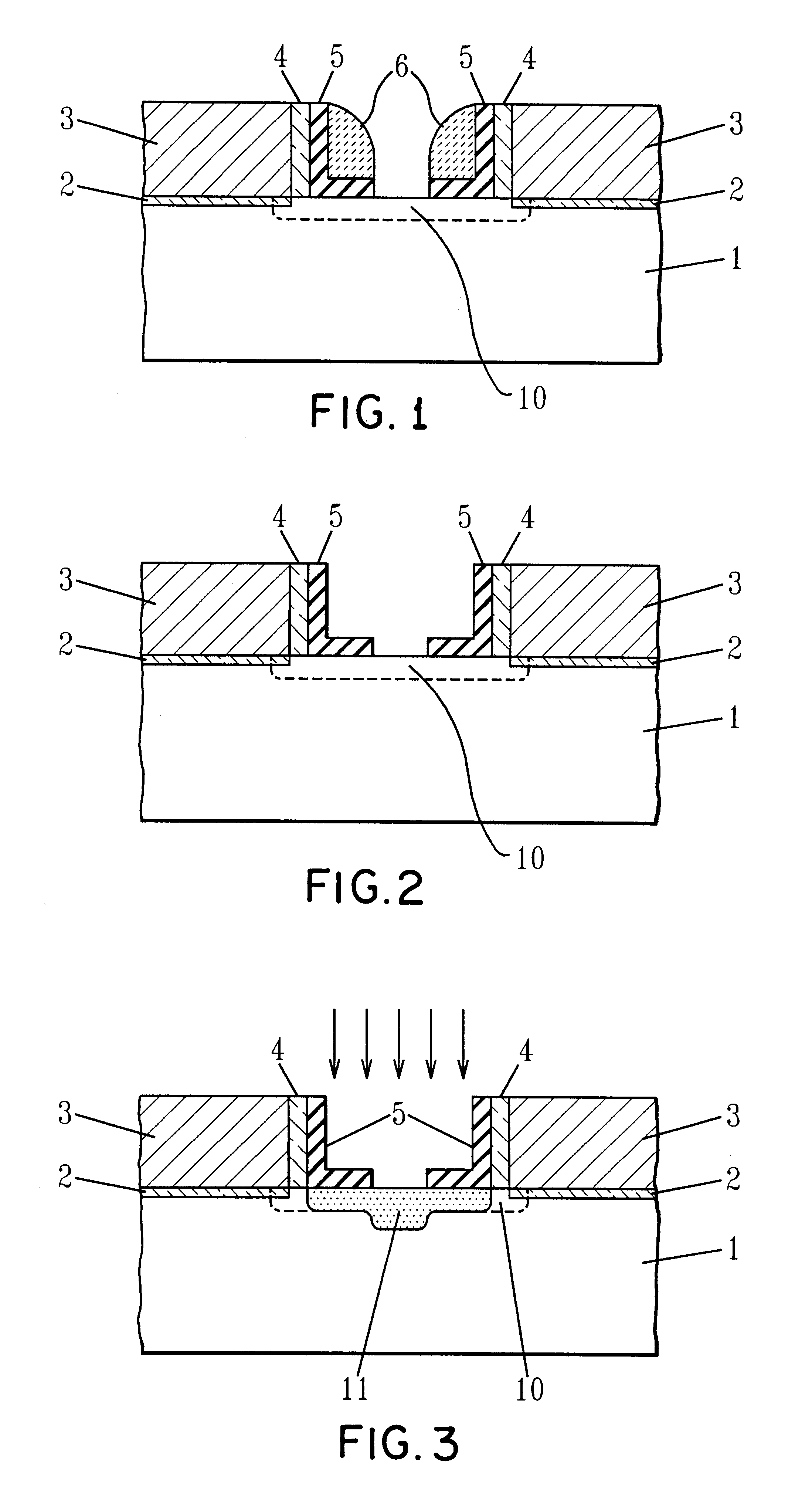
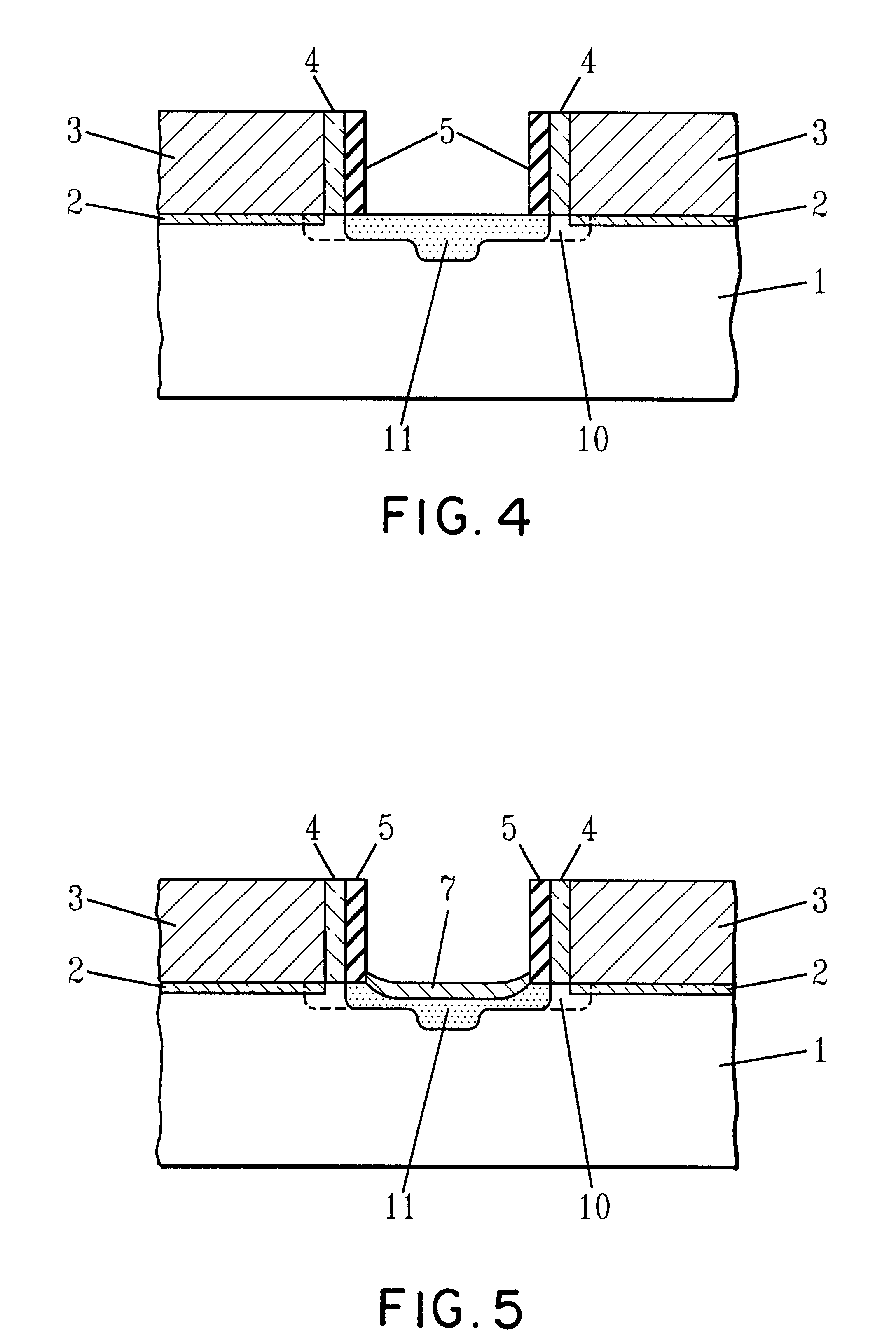
In order to facilitate an understanding of the present invention, reference will be made to the various figures. The present invention provides a method for increasing the space available for silicide formation between adjacent gate structures thereby lowering the diffusion resistance. The method of the present invention permits effectively increased spacing for silicide formation without degrading the device short channel behavior.

In particular, according to the present invention, a semiconductor substrate 1 and gate conductor 3 located above gate insulator 2 is provided. The semiconductor substrate is typically silicon and the gate insulator 2 is typically silicon dioxide. A typical gate conductor 3 is a doped polycrystalline silicon, often referred to simply as polysilicon.

The thin gate insulator 2 is typically grown on or deposited onto the substrate 1. The gate insulator is typically about 30 to about 100 .ANG. thick and can be formed by thermal oxidation of the silicon substra...


PUM


Abstract

A semiconductor structure comprising a plurality of gates located on a semiconductor substrate; wherein insulating spacer is provided on sidewalls of the gates; and metallic silicide located between the gates is provided along with a method for its fabrication. A partially disposable spacer permits increased area for silicide formation without degrading the device short channel behavior.

Description

The present invention relates to a semiconductor structure having metallic silicide in source / drain regions and especially source / drain regions between closely spaced gate structures. In particular, the present invention includes forming an L-shaped spacer between adjacent gate structures. The L-shaped spacer is used to form shallow source / drain regions adjacent to the gates, independent of the lightly doped drain regions (LDDs). The L-shaped spacer is subsequently modified to increase the available area for silicide formation without the silicide directly contacting the lightly doped drain regions.BACKGROUND OF INVENTIONIn fabricating semiconductor structures, the source / drain resistance is reduced by forming a layer of a refractory metal silicide. In particular, a refractory metal is deposited and then subjected to elevated temperatures, thereby reacting with underlying silicon to form what is commonly referred to as a "silicide". Silicides are well known in the art and provide de...

Claims


Application Information

Patent Timeline
IPC IPC(8): H01L21/336H01L29/78H01L21/02H01L29/66H01L29/08H01L21/266H01L29/02
CPCH01L29/6653H01L29/6656H01L29/6659H01L29/7833H01L21/266H01L29/0847
Inventor MILES, GLEN L.
Owner IBM CORP
Why Eureka
Try Eureka