Method for fabricating dynamic random access memory cells

a technology of dynamic random access and memory cells, which is applied in the direction of semiconductor devices, electrical devices, transistors, etc., can solve the problems of soft errors, transfer gate pitch works against the integration of memory cells, and the content of memories is ruined

Inactive Publication Date: 2001-07-31
HYUNDAI ELECTRONICS IND CO LTD
View PDF2 Cites 45 Cited by
  • Summary
  • Abstract
  • Description
  • Claims
  • Application Information

AI Technical Summary

Problems solved by technology

The decrease in the amount of charges results in soft errors that may destroy the content of memories.
Such increase in transfer gate pitch works against the integration of the memory cell.
Another problem lies in that soft errors occur due to a parasitic capacitance, since the capacitor of memory cell adjoins the peripheries and the top portion of the bit lines.

Method used


Image

  • Method for fabricating dynamic random access memory cells
  • Method for fabricating dynamic random access memory cells
  • Method for fabricating dynamic random access memory cells

Examples


Embodiment Construction

Hereinafter, the present invention will be described in detail with reference to the accompanying drawings.

FIG. 3 is a plan view of a memory cell array of a DRAM according to the present invention.

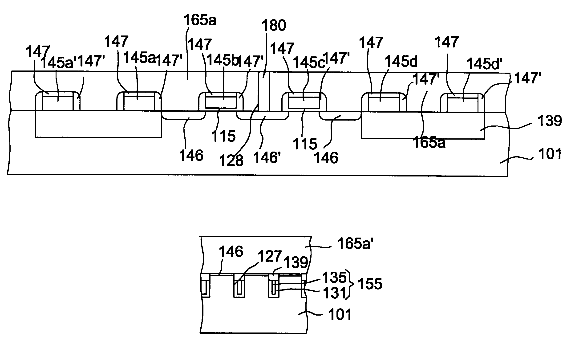
Referring to FIG. 3, in the surface of a semiconductor substrate 101 are formed a plurality of word lines 145a', 145a, 145b, 145c, 145d and 145d' which run parallel with one another in rows, a plurality of bit lines 155 which run parallel with one another in columns, and a plurality of memory cells (MC) arranged at the nearest intersections of the word line and the bit lines. Each memory cell comprises one transfer gate transistor 153 and one capacitor 164 connected thereto. The transfer gate transistor 153 comprises a pair of source / drain regions 146 and 146 formed in the surface of the semiconductor substrate 101, and gate electrodes (word lines) 145b and 145c formed between the source / drain regions 146 and 146 with a gate insulation layer 115 interposed therebetween. A thick insulation ...


PUM


Abstract

A method for fabricating DRAM cells according to the present invention includes the steps of: forming a trench within a semiconductor substrate using a stacked layer as a mask, said stacked layer composed of a silicon oxide film and a silicon nitride film formed in an active region of said semiconductor substrate; forming a first insulation layer on a bottom and sides of said trench; depositing a first conductive layer on whole surface of said semiconductor substrate including said trench; etching back said conductive layer to be recessed from a top surface of said semiconductor substrate and forming bit lines of said first conductive layer on said bottom of said trench in a direction of column; filling a second insulation layer in said trench; removing said stacked layer and a part of said second insulation layer to expose said semiconductor substrate in said active region and planarizing said semiconductor substrate simultaneously; forming a gate insulation layer on said semiconductor substrate;forming a gate structure of a second conductive layer on said gate insulation layer; forming a spacer of an insulation layer on said sides of said gate structure of said second conductive layer; forming source and drain regions on both sides of said gate structure of said second conductive layer;forming a third insulation layer on said semiconductor substrate; connecting said bit lines to a first one of said source and drain regions with a plug of a third conductive layer filled in a contact hole inside said third insulation layer and said second insulation layer; forming a storage node electrode connected to a second one of said source and drain regions; andforming a plate electrode overlying a dielectric layer disposed said storage node electrode.Accordingly, the present invention has the buried bit lines in the trench, making it easy to secure a process margin in the subsequent process, maintaining a constant width of the bit lines to lower the resistance thereof. Furthermore, the bit lines disposed under the word lines has an advantage over patterning the node contact due to the low step height, with enhanced capacitance of the capacitor.

Description

1. Field of the InventionThe present invention relates to a method for fabricating a dynamic random access memory (DRAM) cells and, more particularly, to a DRAM cells provided with a word line on bit line (WOB) type memory cell including a buried bit line structure.2. Discussion of Related ArtA metal-oxide-semiconductor (MOS) type DRAM has a memory cell comprising one MOS transistor and one capacitor connected thereto. As developments have been made in DRAM device technique to achieve high integration and high speed response, each capacitor is shrunken to be of such a reduced size that the amount of charges stored in the capacitor is decreased. The decrease in the amount of charges results in soft errors that may destroy the content of memories. To overcome this problem, a method for increasing the occupied area of each capacitor has been proposed, in which storage nodes composed of polysilicon are formed in a semiconductor substrate in order to increase capacitance of the capacitor...

Claims


Application Information

Patent Timeline
Patent Type & Authority Patents(United States)
IPC IPC(8): H01L21/70H01L21/8242H01L27/108H01L21/77
CPCH01L27/10885H01L27/10814H01L27/10888H10B12/315H10B12/485H10B12/482H01L21/77
Inventor PARK, SYUNG-HYUN
Owner HYUNDAI ELECTRONICS IND CO LTD
Why Eureka
Try Eureka