Method and system for dicing wafers, and semiconductor structures incorporating the products thereof

Inactive Publication Date: 2001-08-07
IBM CORP
View PDF23 Cites 127 Cited by
  • Summary
  • Abstract
  • Description
  • Claims
  • Application Information

AI Technical Summary

Problems solved by technology

Small-scale damage is associated with large strength (strong chips or chip-edges, capable of sustaining large stresses) and large-scale damage is associated with small strength (weak chips or chip-edges, capable of sustaining only small stresses).
This leads to loss of devices on packaging or expensive, more compliant package re-designs.
This is not possible with conventional front face dicing, such as illustrated in FIG.
In cases in which the entire chip experiences significant tension, there is an analogous need for entrance cuts on both sets of edges, and, again this is not possible with conventional front face dicing.
From a practical standpoint, such a procedure

Method used


Image

  • Method and system for dicing wafers, and semiconductor structures incorporating the products thereof
  • Method and system for dicing wafers, and semiconductor structures incorporating the products thereof
  • Method and system for dicing wafers, and semiconductor structures incorporating the products thereof

Examples


Embodiment Construction

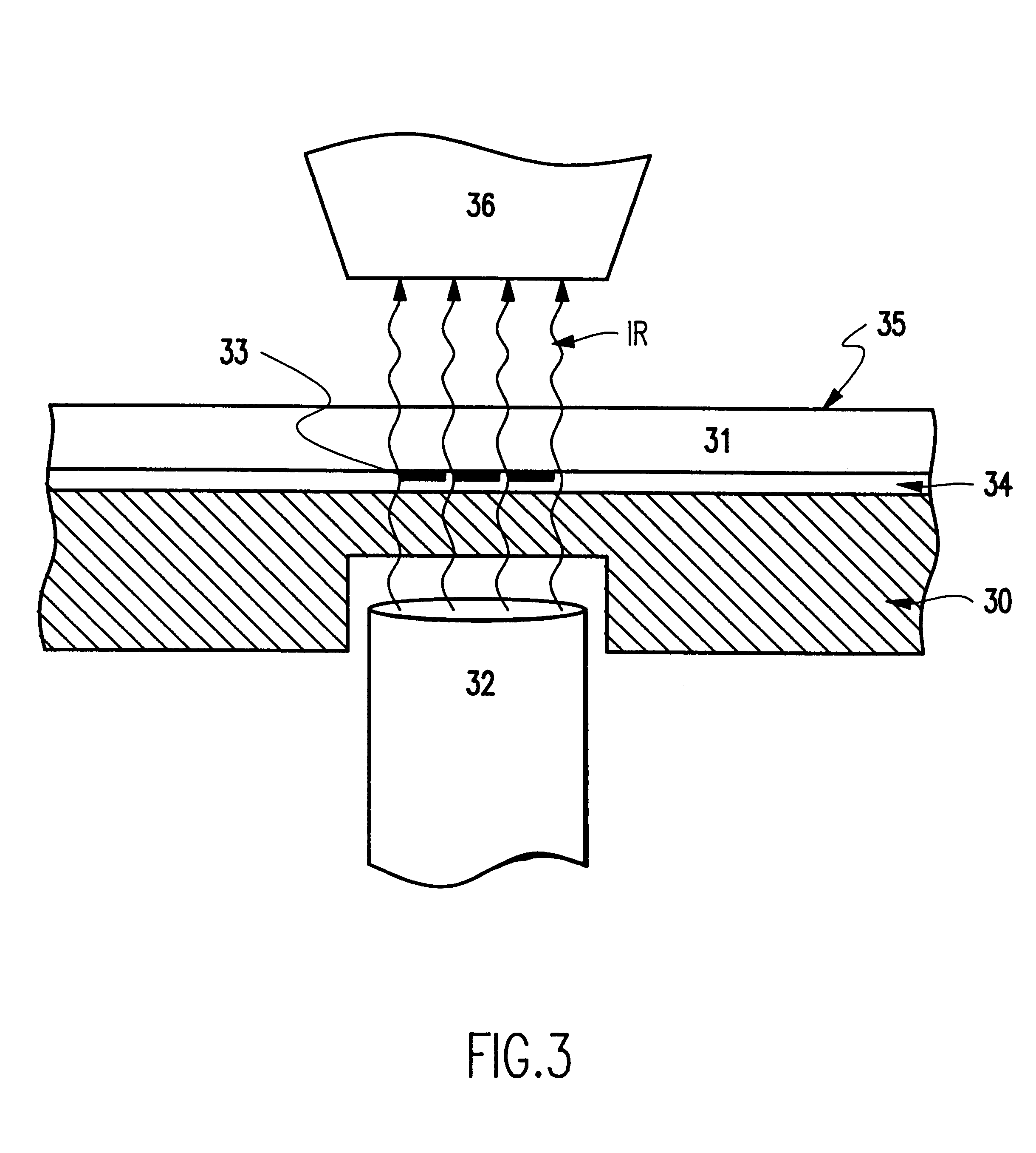
With reference to the figures, and particularly FIG. 3, a dicing chuck or jig 30 is used to support a transparent semiconductor wafer 31 to be diced into individual chips or die units. The wafer is releasably mounted to the chuck with conventional wafer dicing tape (not shown). The semiconductor wafer 31 is transparent to the wavelength of light to be used to illuminate a non-light transparent (opaque) dicing alignment pattern 33 formed on the front side 34 of the wafer 31. The front side 34 of the wafer has the active circuitry. Where the semiconductor wafer 31 is silicon, it is useful to employ infrared (IR) light as the illuminating light. Infrared radiation generally has a wavelength of greater than 700 nm. The silicon wafer is transparent to, i.e., transmits, infrared light of this wavelength.

An optical assembly used includes an optical fiber 32 used to align cuts to be later formed in the wafer back side 35 with non-transparent (to IR) alignment marks patterned onto the front ...


PUM

PropertyMeasurementUnit
Thicknessaaaaaaaaaa
Structureaaaaaaaaaa
Transparencyaaaaaaaaaa

Abstract

A method and system for dicing a semiconductor wafer providing a structure with greatly reduced backside chipping and cracking, as well as increased die strength. Semiconductor chip structures obtained from wafers diced according to this invention are also encompassed.

Description

1. Field of the InventionThe invention relates to a method and system for dicing wafers of greater die strength, and semiconductor structures incorporating the products thereof.2. Description of the Related ArtThin semiconductor wafers have been separated into a plurality of diced chips by a number of conventional techniques including sawing, laser scribing, mechanical scribing and cleaving, and chemical etching and cleaving.Referring to FIG. 1, the dicing of a wafer by sawing is illustrated in which a diamond saw blade 10 is shown with its rotational and lateral directions of motion indicated by arrows. The blade 10 has a forward entrance edge 14 cutting through the active (upper) face 12 of the semiconductor wafer 11 and an exit edge 15 at the back (bottom) side 13 of the wafer 11. Dicing striations 16 formed through the thickness of the wafer 11 by action of the sawing blade 10 are indicated. Referring now to FIGS. 2A and 2B, when a thin semiconductor wafer 10 is sawed in this ma...

Claims


Application Information

Patent Timeline
IPC IPC(8): B23D59/00B28D5/00B28D5/02H01L21/02H01L21/70H01L21/607H01L21/78H01L21/301H01L29/06
CPCB23D59/002B28D5/022H01L21/78H01L24/85H01L2924/10253H01L2924/014H01L2924/01033H01L29/0657H01L2224/16H01L2224/48091H01L2224/48247H01L2224/4826H01L2224/78302H01L2224/85H01L2924/01002H01L2924/01006H01L2924/01014H01L2924/01018H01L2924/01027H01L2924/01075H01L2924/01077H01L2924/01082H01L2924/10158H01L2924/14H01L2924/01005H01L2924/01023H01L2924/00014H01L2924/00H01L24/48H01L2924/10155H01L2924/12042Y10T83/0259Y10T83/0378Y10T83/0581H01L2224/45099H01L2224/05599
Inventor BROUILLETTE, DONALD W.COOK, ROBERT F.FERENCE, THOMAS G.HOWELL, WAYNE J.LINIGER, ERIC G.MENDELSON, RONALD L.
Owner IBM CORP
Why Eureka
Try Eureka