

Process for forming a low resistivity titanium silicide layer on a silicon semiconductor substrate and the resulting device
a technology of titanium silicide and silicon semiconductor, which is applied in the direction of semiconductor devices, semiconductor device details, electrical equipment, etc., can solve the problems of reducing the performance of the semiconductor device (e.g., the cmos device) being produced, and becoming increasingly difficult to use thermal annealing to transform a structure,
- Summary
- Abstract
- Description
- Claims
- Application Information
AI Technical Summary
Problems solved by technology
Method used
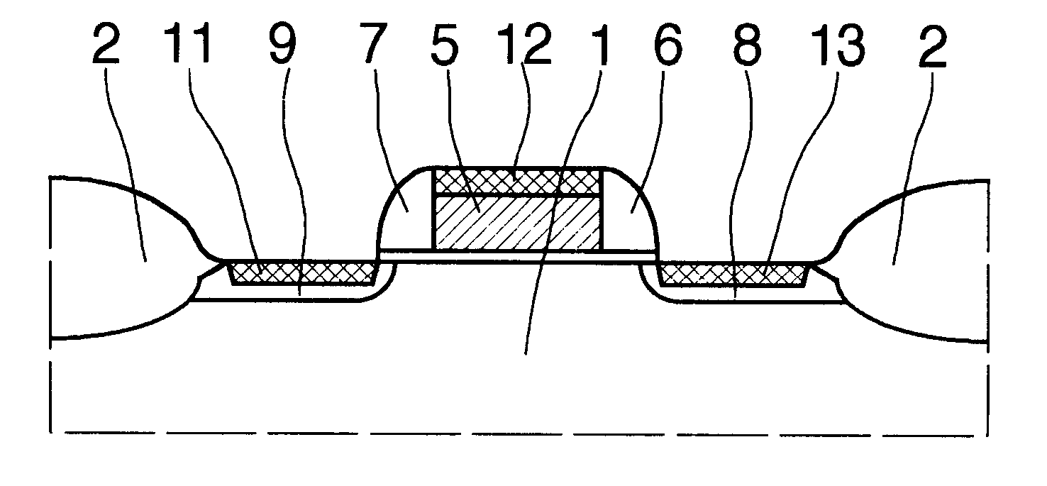
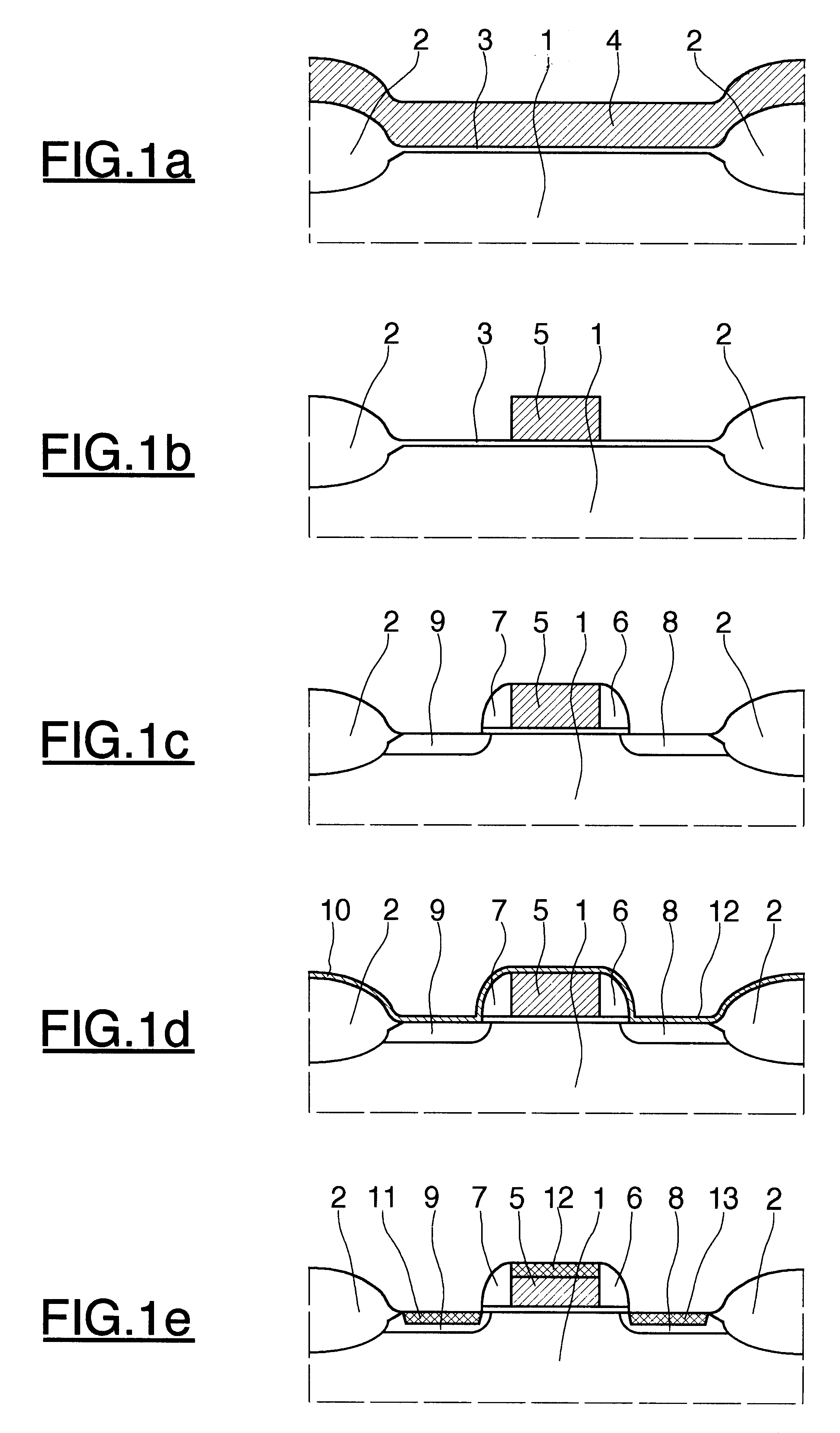
Image

Examples
example 4
5. Example 4
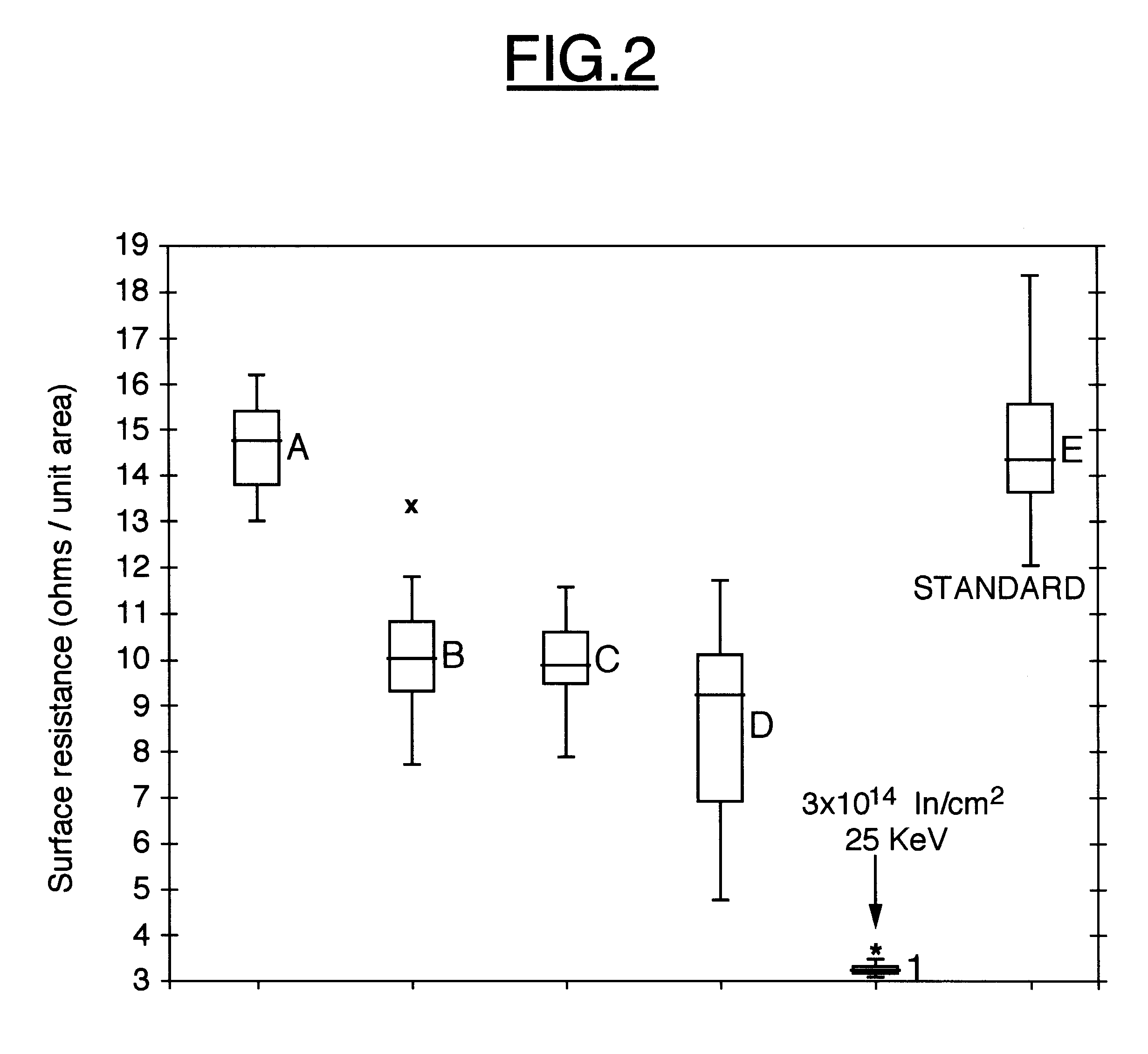
A 40 nm titanium layer and a 25 nm titanium nitride layer were deposited on monocrystalline silicon wafers. Before the deposition, some of the wafers "In" underwent indium implantation in accordance with the present invention at an implantation energy of 25 keV and at an implantation level of 10.sup.14 atoms / cm.sup.2, and other wafers "Ref" were not subjected to indium implantation. The resulting wafers were subjected to a rapid thermal annealing operation at various temperatures, and the surface resistances of the titanium silicides that were produced was measured. As shown in FIG. 8, when the indium implantation process of the present invention was used, silicide formation took place at temperatures that were approximately 50.degree. C. below those required to obtain the same surface resistance when the wafer was not subjected to indium implantation.
PUM
 Abstract
Description
Claims
Application Information