Static random access memory (RAM) systems and storage cell for same

a random access memory and storage cell technology, applied in static storage, information storage, digital storage, etc., can solve the problems of requiring more space on a semiconductor chip, requiring less power, and reducing the storage capacity of the chip

Inactive Publication Date: 2001-10-09
ORACLE INT CORP
View PDF3 Cites 21 Cited by
  • Summary
  • Abstract
  • Description
  • Claims
  • Application Information

AI Technical Summary

Problems solved by technology

Static cells are generally faster, consume less power and have lower error rates, but have the disadvantage of requiring more space on a semiconductor chip.
Unfortunately, this charge gradually leaks off and, if the cell is not accessed for a period of time, the cell is likely to lose its logic state.
This is effective, but it increases

Method used


Image

  • Static random access memory (RAM) systems and storage cell for same
  • Static random access memory (RAM) systems and storage cell for same
  • Static random access memory (RAM) systems and storage cell for same

Examples


first embodiment

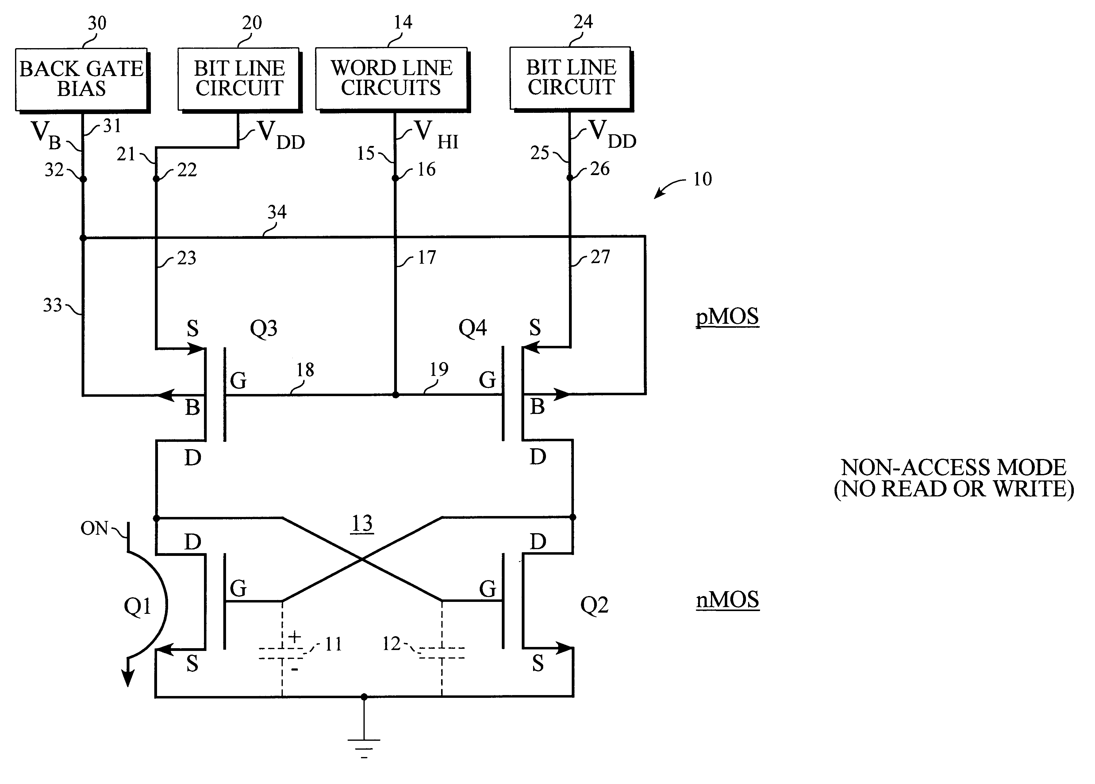
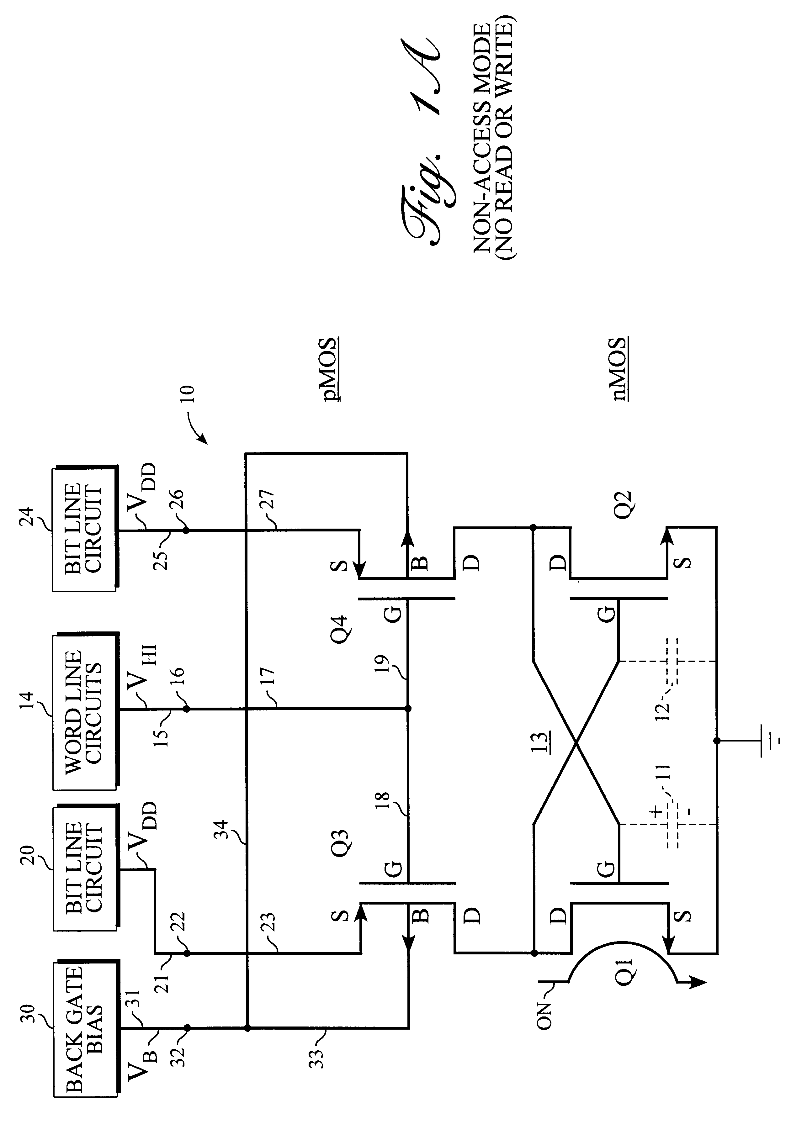
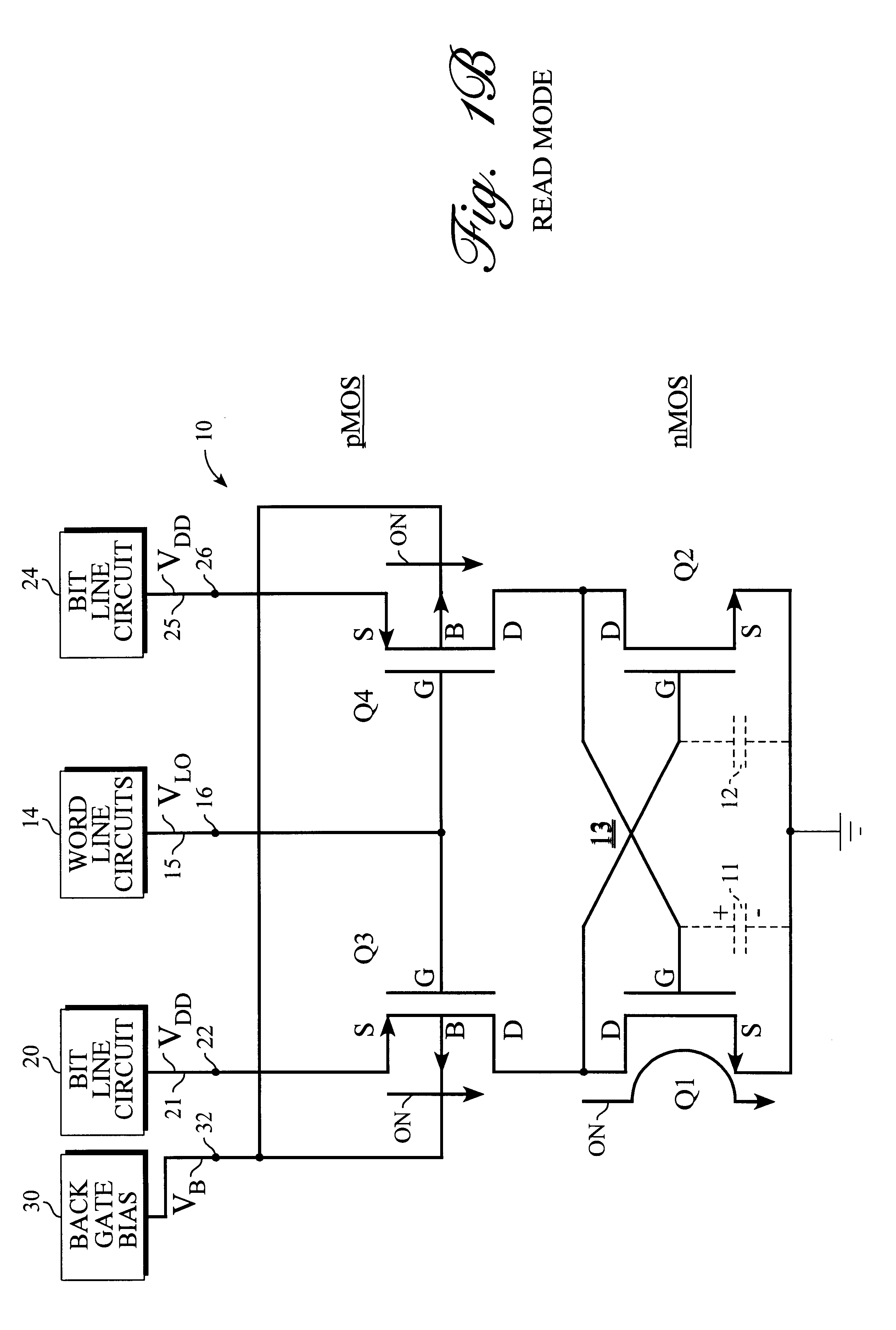
Referring to FIG. 1A, there is shown a static RAM (random access memory) storage cell 10 constructed in accordance with the present invention. Storage cell 10 is a four-transistor storage cell comprising transistors Q1, Q2, Q3 and Q4. In the present embodiment, each of these transistors is a metal oxide semiconductor (MOS) type field effect transistor (FET). Each of transistors Q1-Q4 includes a source terminal S, a drain terminal D and a gate terminal G. Each of these transistors also includes a fourth terminal, namely, a back gate terminal B that is comprised of the body or substrate of the transistor. This back gate terminal is usually not mentioned and is usually not shown in circuit diagrams. This back gate terminal B is usually assumed to be connected internally to the source terminal S or to the appropriate power supply circuit and is normally not discussed in connection with the operation of the transistor. This back gate terminal B, however, can be of value and is used by th...

second embodiment

Referring now to FIG. 5 of the drawings, there is shown a static RAM storage cell 40 constructed in accordance with the present invention. In this embodiment, the channel types for the storage transistors and the bit line coupling transistors are reversed. In particular, FIG. 5 shows a pair of storage transistors Q5 and Q6, which are cross-coupled to form a bistable circuit 41. In this case, storage transistors Q5 and Q6 are p-channel MOS field-effect transistors. The storage cell 40 further includes first and second bit line coupling transistors Q7 and Q8 individually connected in series with the different ones of the first and second storage transistors Q5 and Q6. In the FIG. 5 case, the bit line coupling transistors Q7 and Q8 are n-channel MOS field-effect transistors. The voltages shown in FIG. 5 are for the non-access or standby mode.

A word line circuit 42 supplies access and non-access voltages to the normal gate terminals G of coupling transistors Q7 and Q8. The non-access vo...


PUM


Abstract

A method of continuously replenishing a four-transistor static RAM storage cell is described. Such method comprises biasing both the back gate terminals and the normal gate terminals of the two bit line coupling transistors in the static RAM storage cell to voltage levels for causing a flow of small compensating currents through such coupling transistors when they are in a standby or non-access condition. Such small compensating currents are supplied to the two storage transistors in the storage cell for replenishing leakage of charge from the parasitic capacitance in the storage cell. The bias voltages arc supplied by adaptive bias circuits which adjust the bias voltages to track changes in the leakage of charge from the parasitic cell capacitance.

Description

DESCRIPTION1. Technical FieldThis invention relates to digital memory cells and memory systems. More particularly, it relates to static-type semiconductor random access memory (RAM) storage cells and systems.2. Background of the InventionVarious forms of static and dynamic semiconductor storage cells are known in the art. Static cells continue to store data for as long as power is applied to them. In contrast, a dynamic storage cell must be periodically refreshed or it loses the data stored in it. Static cells are generally faster, consume less power and have lower error rates, but have the disadvantage of requiring more space on a semiconductor chip.As is known, semiconductor storage cells rely on the charge on a parasitic cell capacitance to maintain the state of the cell when it is not being accessed. Unfortunately, this charge gradually leaks off and, if the cell is not accessed for a period of time, the cell is likely to lose its logic state. Dynamic cells solve this problem by...

Claims


Application Information

Patent Timeline
IPC IPC(8): G11C11/412G11C8/08G11C8/00G11C11/417
CPCG11C8/08G11C11/412G11C11/417
Inventor ANG, MICHAEL ANTHONYHEALD, RAYMOND A.LO, ROGER Y.
Owner ORACLE INT CORP
Why Eureka
Try Eureka