

Fabrication method for semiconductor device utilizing parallel alignment slits
a technology of parallel alignment and semiconductor devices, which is applied in the direction of semiconductor/solid-state device testing/measurement, semiconductor/solid-state device details, instruments, etc., can solve the problems of giving the overlay error degree, the reading or recognition of upper and lower alignment marks with the optical microscope is difficult, and the overlay error degr
- Summary
- Abstract
- Description
- Claims
- Application Information
AI Technical Summary
Problems solved by technology
Method used
Image

Examples
first embodiment
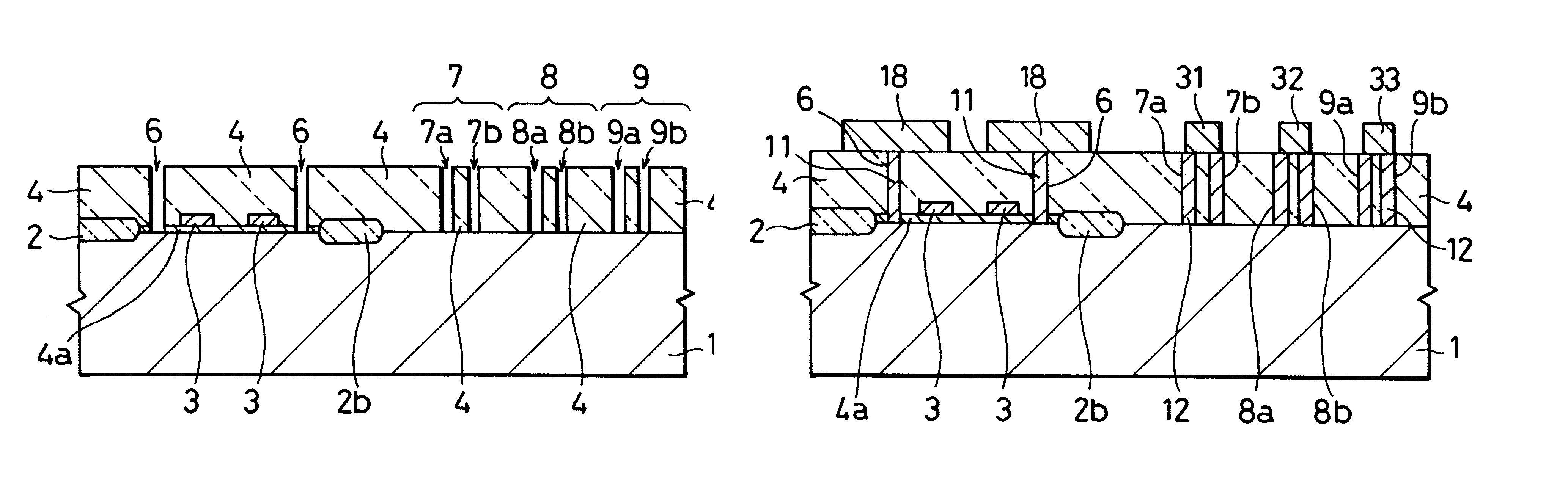
A fabrication method for a semiconductor device, i.e., a DRAM, is shown in FIGS. 6A to 6G.
First, as shown in FIG. 6A, a field oxide layer 2 is selectively formed on a main surface of a silicon substrate 1 by a selective oxidation process or the like, thereby defining active regions. For the sake of simplification of description, only one of the active regions is shown in FIG. 6A to 6G, which active region is for a MOSFET.
Then, a gate oxide layer 4a is selectively formed on the exposed surface of the substrate 1 in the active region. Gate electrodes 3 are formed on the gate oxide layer 4a in the active regions. Source / drain regions (not shown) are formed in the active region of the substrate 1. Thus, two MOSFETs are formed in the active region as transfer transistors of the memory cell. These steps are performed by known processes.
Further, a SiO.sub.2 layer with a thickness of approximately 800 nm is formed on the whole substrate 1 to cover the MOSFETs by a CVD process or the like. ...
second embodiment
A fabrication method of a semiconductor device according to a second embodiment is shown in FIGS. 10 and 11, in which outer and inner alignment box marks for the automatic overlay measurement are used.
As shown in FIGS. 10 and 11, four slits 33, 34, 35, and 36 are formed so as to define a square shape in the interlayer insulating layer 4 formed on the silicon substrate 1. The substrate 1 and the interlayer insulating layer 4 are the same as those in the first embodiment. The slits 33, 34, 35, and 36 serve as the outer alignment box mark.
The opposing slits 33 and 34 are arranged in parallel at a pitch P3. The opposing slits 35 and 36 are arranged in parallel at the same pitch P3, and perpendicular to the slits 33 and 34. The four slits 33, 34, 35, and 36 have the same width of W3 and the same length L3. The width W3 is, for example, set to approximately 0.5 .mu.m. The length L3 is suitably determined as necessary.
The slits 33, 34, 35, and 36 are filled with a suitable conductive or in...
third embodiment
A fabrication method of a semiconductor device according to a third embodiment is shown in FIG. 12.
In the above first and second embodiments, the present invention is applied to the overlay measurement of the lower electrodes of the storage capacitors with respect to the underlying contact holes in the DRAM memory cell. In these embodiments, the edges of the slits formed in the interlayer insulating layer 4 provide the main scale of the vernier caliper, and the edges of the resist pattern or patterns formed in the resist layer provide the vernier scale thereof.
However, the present invention may be applied to the well-known trench isolation structure, as shown in the third embodiment explained below.
The fabrication method according to the third embodiment is substantially the same as that according to the first embodiment, except that the slits in the interlayer insulating layer are formed in a semiconductor substrate.
First, as shown in FIG. 12, a patterned masking layer (not shown) ...
PUM
 Abstract
Description
Claims
Application Information