

High selectivity Si-rich SiON etch-stop layer
a si-rich sion, high selectivity technology, applied in the direction of basic electric elements, semiconductor/solid-state device manufacturing, electric devices, etc., can solve the problems of distorted photoresist patterns, increased photolithographic patterning problems, and many of these materials cannot be used, and achieve high selectivity of si-rich sion
- Summary
- Abstract
- Description
- Claims
- Application Information
AI Technical Summary
Problems solved by technology
Method used
Image

Examples
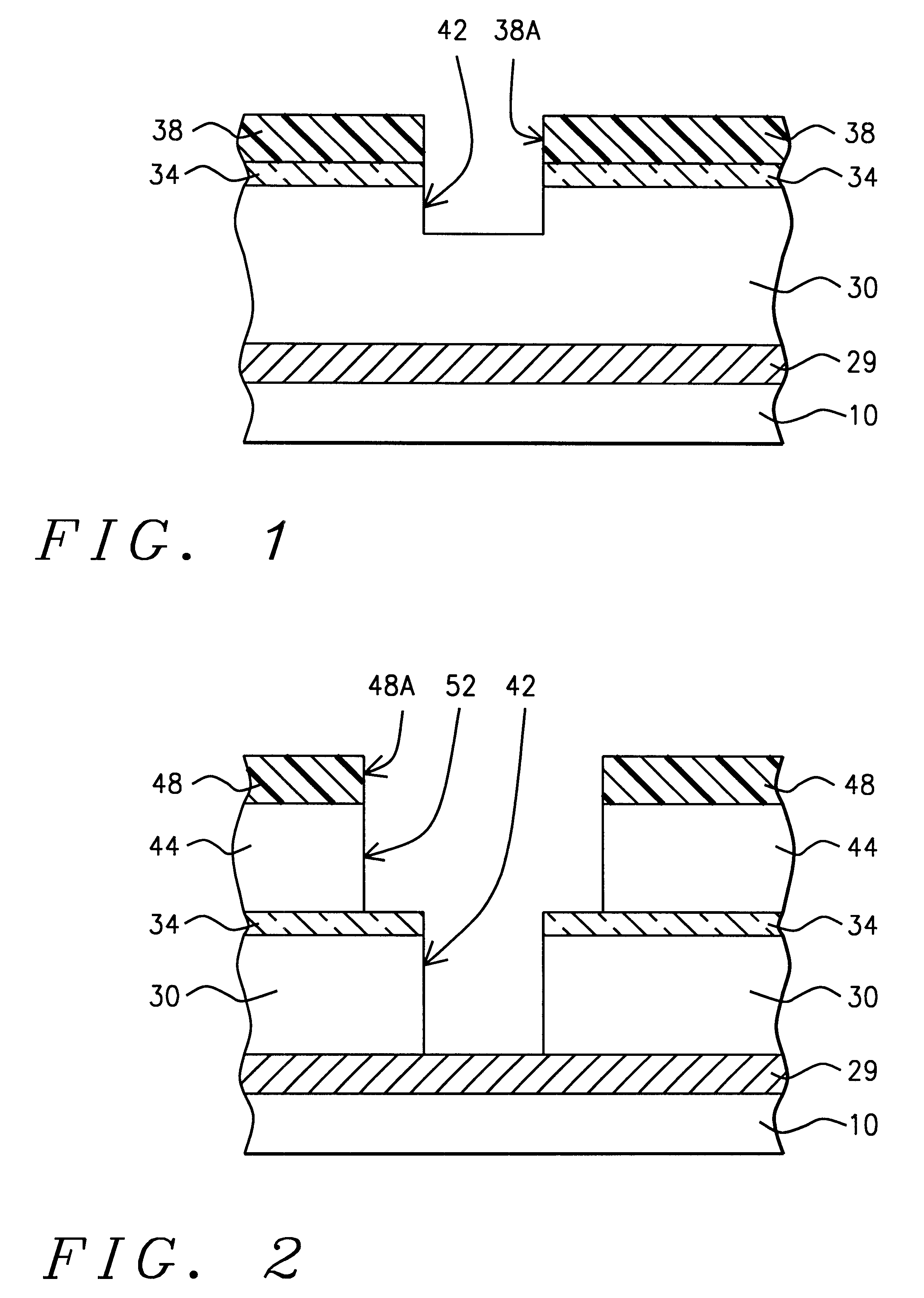
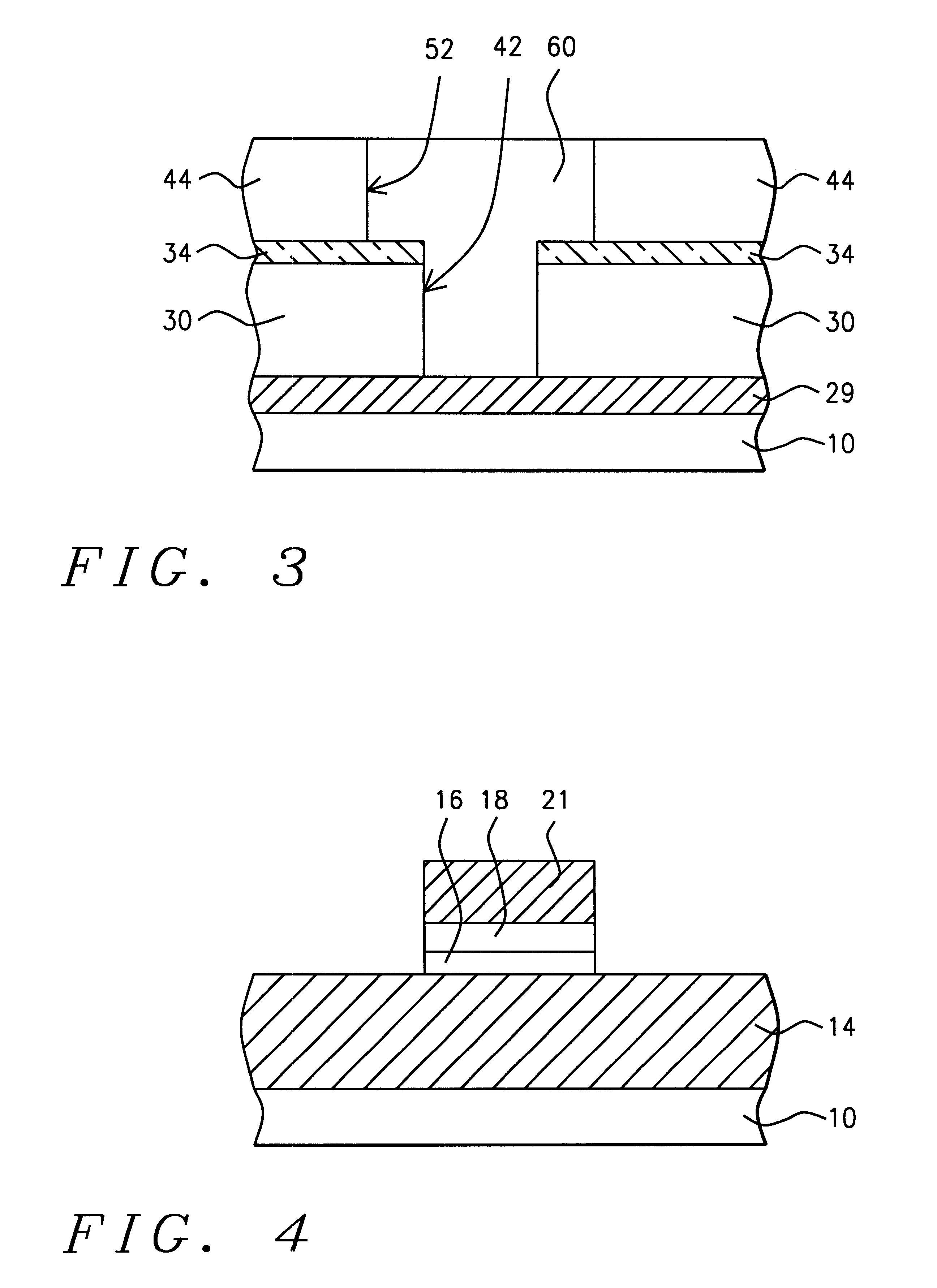
first embodiment
The first embodiment is shown in FIGS. 1 to 3. To begin, a conductive structure 29 of some type is formed over the substrate or semiconductor structure 10. The conductive structure can be a conductive line. The conductive line can preferably be an Al alloy or Cu alloy line. The semiconductor structure can comprise a wafer, with doped regions formed therein and with gates and other devices formed thereon or thereovcr. An insulating layer can be formed over the wafer and the conductive line can be formed over the insulating layer.
Subsequently, we form a first insulating layer (IMD) 30 over the conductive line 29. The first insulating layer 30 preferably bas a thickness of between about 5000 and 10,000 A The first insulating layer is preferably composed of Silicon oxide.
C. invention's Si Rich SiON ARC Etch Stop Layer 34
In a key step, the invention's key Si Rich SiON ARC etch stop layer 34 over the first insulating layer 30. A major advantage of the invention is that the ARC Si rich SiO...
second embodiment
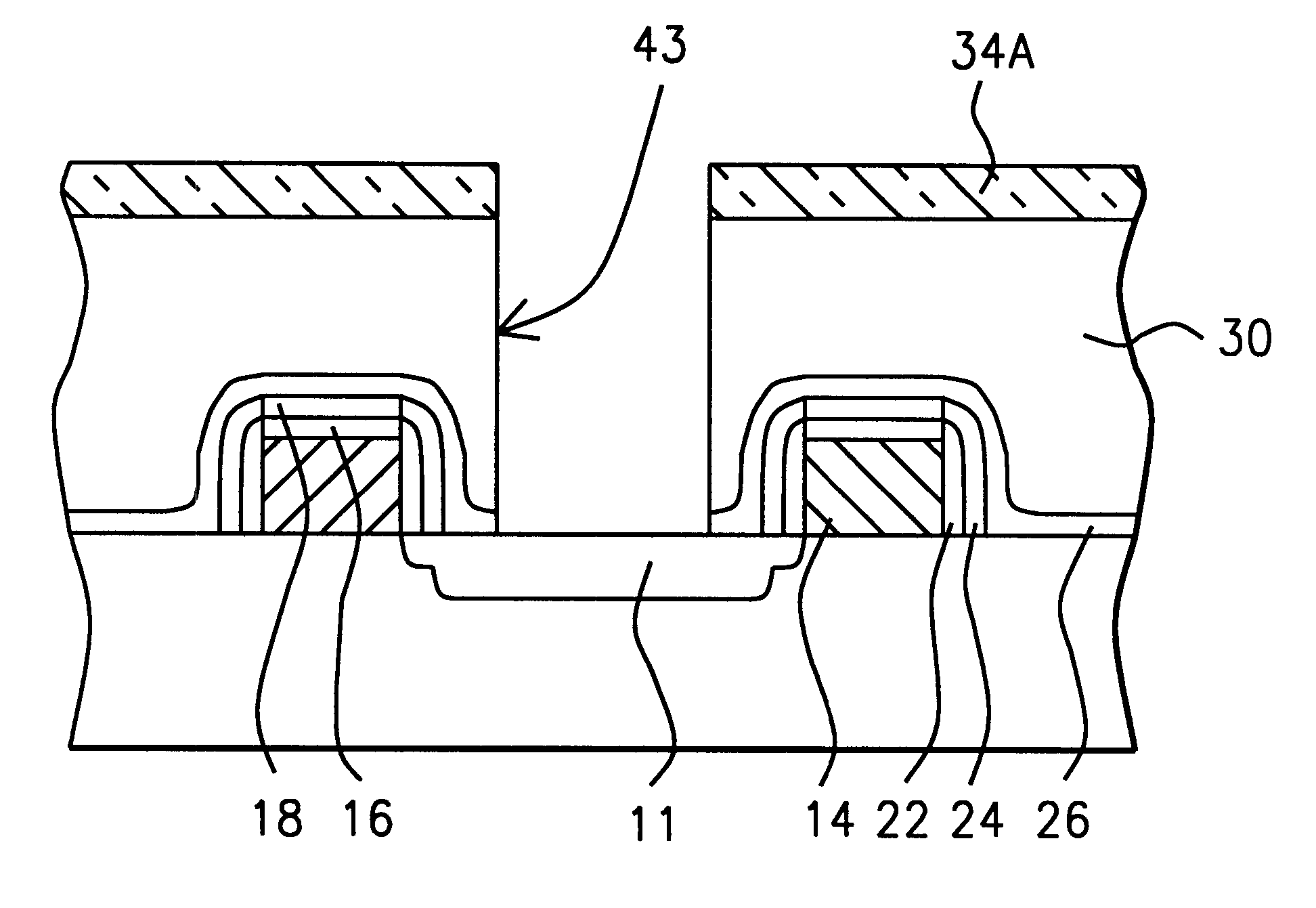
--SAC WITH HARD MASK AND SPACERS FORMED OF Si Rich SiON
A. Overview of the Second Embodiment
FIGS. 4 through 8 show a preferred 2.sup.nd embodiment where a self aligned contact (SAC) is formed using special Si Rich Silicon oxynitride spacer layers on the gate electrode 14 and a Si Rich SiON hard mask 18.
The key aspects of the invention for the 2.sup.nd embodiment are:
Si rich SiON top hard mask layer 18 and Si rich SiON 2.sup.nd spacer 24
oxide etch process to etch oxide layer 30 but is highly selective to the Si rich SiON top hard mask layer 18 and 2.sup.nd spacer 24.
An overview of the major steps of the second embodiment is shown below.
The 2.sup.nd embodiment includes the following steps:
a) form a polysilicon layer over a substrate 10;
b) form a hard mask layer on the polysilicon layer; the hard mask layer 1618 comprised of a bottom hard mask 16 on a Silicon oxynitride hard mask 18;
the silicon oxynitride hard mask 18 is preferably composed of Si-rich SiON having a Si molar percentage b...
PUM
| Property | Measurement | Unit |
|---|---|---|
| Pressure | aaaaa | aaaaa |
| Pressure | aaaaa | aaaaa |
| temperature | aaaaa | aaaaa |
Abstract
Description
Claims
Application Information