One-sided circuit board for multi-layer printed wiring board, multi-layer printed wiring board, and method of its production

a multi-layer printed wiring board and one-sided circuit board technology, applied in the direction of printed element electric connection formation, non-metallic protective coating application, coupling device connection, etc., can solve the problems of inability to meet the requirements of super-miniaturization of portable electric equipment, inability to achieve a high densification of mounting parts, and inability to fully meet the requirements of narrow-pitched packages and mcm. , to achieve the effect of high densification and high den

Inactive Publication Date: 2001-11-20
IBIDEN CO LTD
View PDF8 Cites 85 Cited by
  • Summary
  • Abstract
  • Description
  • Claims
  • Application Information

AI Technical Summary

Problems solved by technology

However, in the multilayer printed wiring board having the above-mentioned through-hole structure, it is required to ensure a region for the formation of the through-holes, so that it is difficult to attain a high densification of mounting parts and hence there are disadvantages that it is not able to fully meet the requirements of super-miniaturization of portable electric equipments and practical application of the narrow-pitched packages and MCM (Multi Chip Module).
The drawback of the above conventional technique is that the production steps become complicated and a long time is taken for the production because the heating and pressing through hot press and the patterning step of the copper foil through etching should be repeated at any number of times.
In the multilayer printed wiring board having the IVH structure obtained by the above production method, it is difficult to confirm the poor patterning of the copper foil in the production course, so that if the poor patterning is caused even at one place (one step) in the production course, the whole of the wiring board as a final product becomes inferior.
That is, the above conventional production process has a fatal drawback that the degradation of production efficiency or production yield is liable to be caused because if inferior good is produced even at one place among the lamination steps, good products made in the other lamination steps should be removed.

Method used


Image

  • One-sided circuit board for multi-layer printed wiring board, multi-layer printed wiring board, and method of its production
  • One-sided circuit board for multi-layer printed wiring board, multi-layer printed wiring board, and method of its production
  • One-sided circuit board for multi-layer printed wiring board, multi-layer printed wiring board, and method of its production

Examples


example

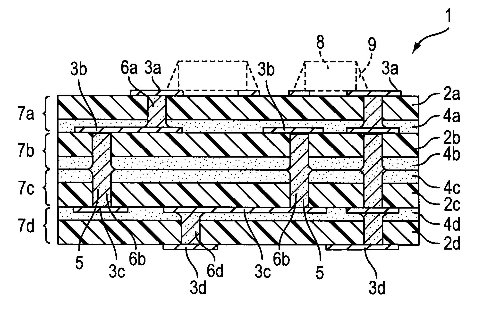
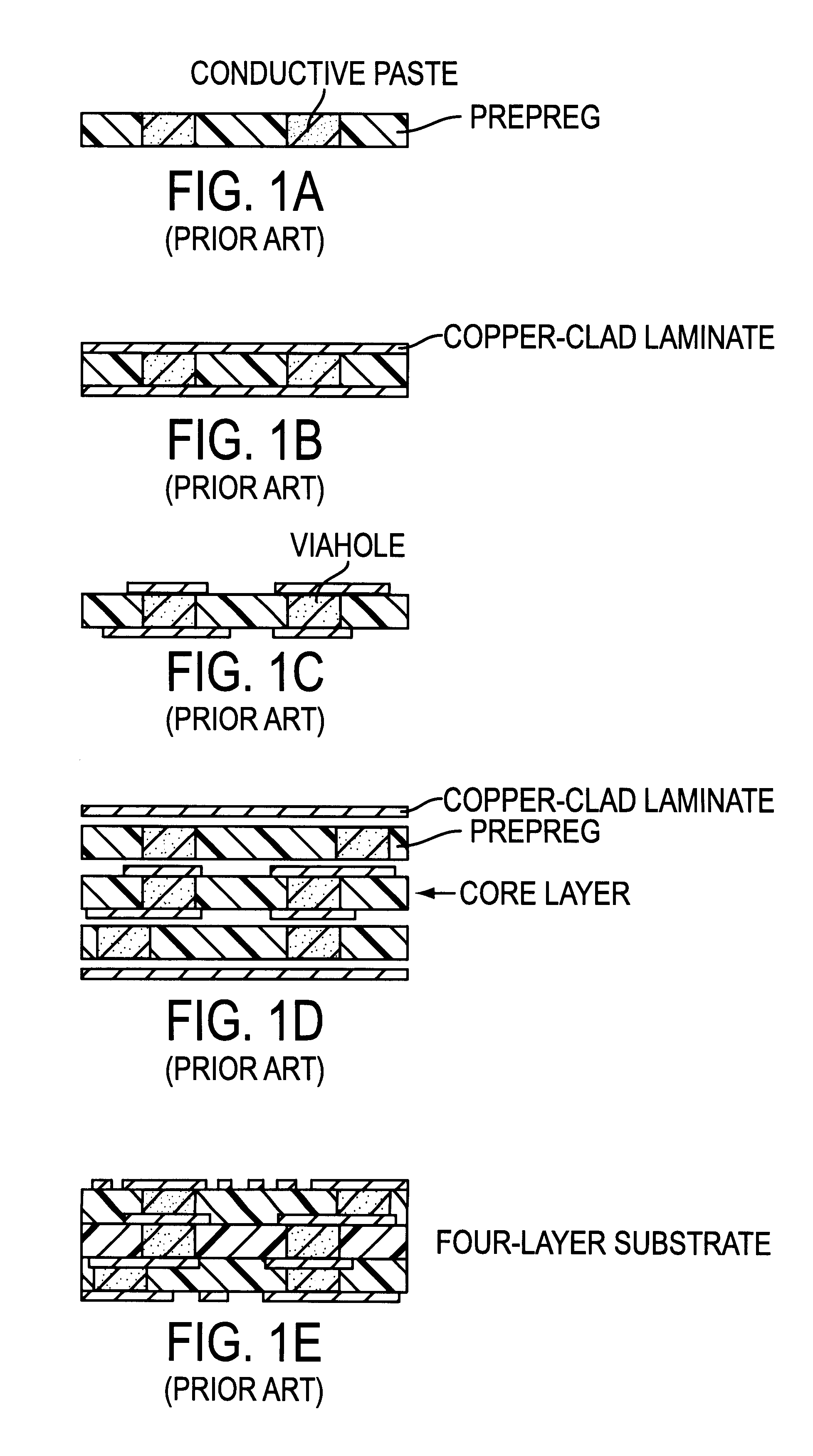
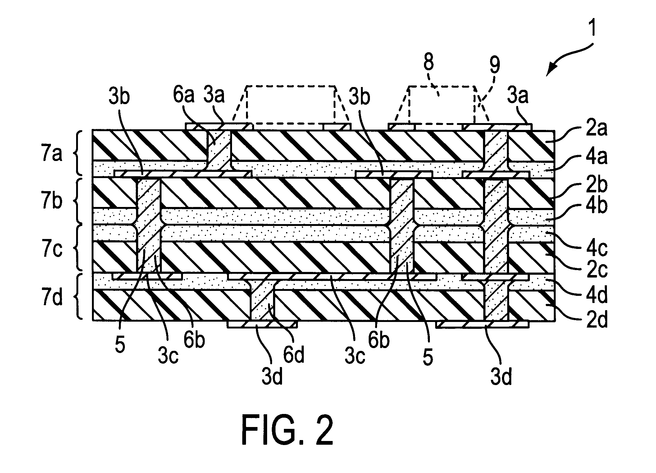
FIG. 2 is a diagrammatically section view of an embodiment of the multilayer printed wiring board according to the invention. In this figure, the multilayer printed wiring board 1 is a four layer board formed by laminating single-sided circuit substrates 7a, 7b, 7c, 7d, which consist of insulating hard substrates 2a, 2b, 2c, 2d and conductor circuits 3a, 3b, 3c, 3d formed by etching a metal foil adhered to a surface of the substrate, adhesive layers 4a, 4b, 4c, 4d each formed on a surface of the substrate opposite to the conductor circuit and viaholes 6a, 6b, 6d formed by filling a conductive paste 5 in holes passing the insulating hard substrates 2a, 2b, 2c, 2d and the adhesive layers 4a, 4b, 4c, 4d and contacting with the conductor circuits 3a, 3b, 3c, 3d, and mutually joining them through the adhesive layers 4a, 4b, 4c, 4d formed on the single-sided circuit substrates 7a, 7b, 7c, 7d, respectively.

In this case, the conductor circuit 3a of the single-sided circuit substrate 7a and ...


PUM

PropertyMeasurementUnit
thicknessaaaaaaaaaa
temperatureaaaaaaaaaa
conductiveaaaaaaaaaa

Abstract

A single-sided circuit substrate for a multilayer printed writing board has an insulating hard substrate, a conductor circuit formed on a surface of the substrate, an adhesive layer formed on the other surface, and at least one viahole through the substrate and the adhesive layer so as to pass these layers and contact with the conductor. The viaholes are filled with conductive paste. The invention also provides a multilayer printed wiring board having an IVH structure constituted with single-sided circuit hard substrates and a method of efficiently manufacturing the same with high yield.

Description

1. Field of the InventionThis invention relates to a single-sided circuit substrate for a multilayer printed wiring board, a multilayer printed wiring board and a method of manufacturing the same, and more particularly, it proposes a single-sided circuit board to be developed for manufacturing a multilayer printed wiring board having an interstitial-viahole structure in higher yield and efficiency, and a multilayer printed wiring board produced by laminating a plurality of such single-sided circuit boards, and a method of manufacturing the same.2. Description of Background InformationThe conventional multilayer printed wiring board is a multilayered body constituted by alternately building up copper-clad laminates and prepregs. This multilayered body has a surface wiring pattern on an outer surface thereof, and has an innerlayer wiring pattern between its interlaminar layers. These wiring patterns are electrically connected via through-holes formed in the multilayered body in a thic...

Claims


Application Information

Patent Timeline
Patent Type & Authority Patents(United States)
IPC IPC(8): H05K3/46H05K3/28H05K3/40
CPCH05K3/4617H05K3/28H05K3/4069Y10T29/49124H05K2201/0195H05K2203/1572
Inventor ENOMOTO, RYO
Owner IBIDEN CO LTD
Why Eureka
Try Eureka