Method of manufacturing liquid crystal display

Inactive Publication Date: 2001-11-27
SHARP KK
View PDF8 Cites 105 Cited by
  • Summary
  • Abstract
  • Description
  • Claims
  • Application Information

AI Technical Summary

Benefits of technology

The present invention was devised to solve the above problems, and therefore, has an object to provide a manufacturing method of an inexpensive active ma

Problems solved by technology

Thus, adhesion between the low-resistance semiconductor film 105 and source metal film 106 becomes poor due to a large interface therebetween, thereby causing problematic film separation between the low-resistance semiconduct

Method used


Image

  • Method of manufacturing liquid crystal display
  • Method of manufacturing liquid crystal display
  • Method of manufacturing liquid crystal display

Examples


embodiment 1

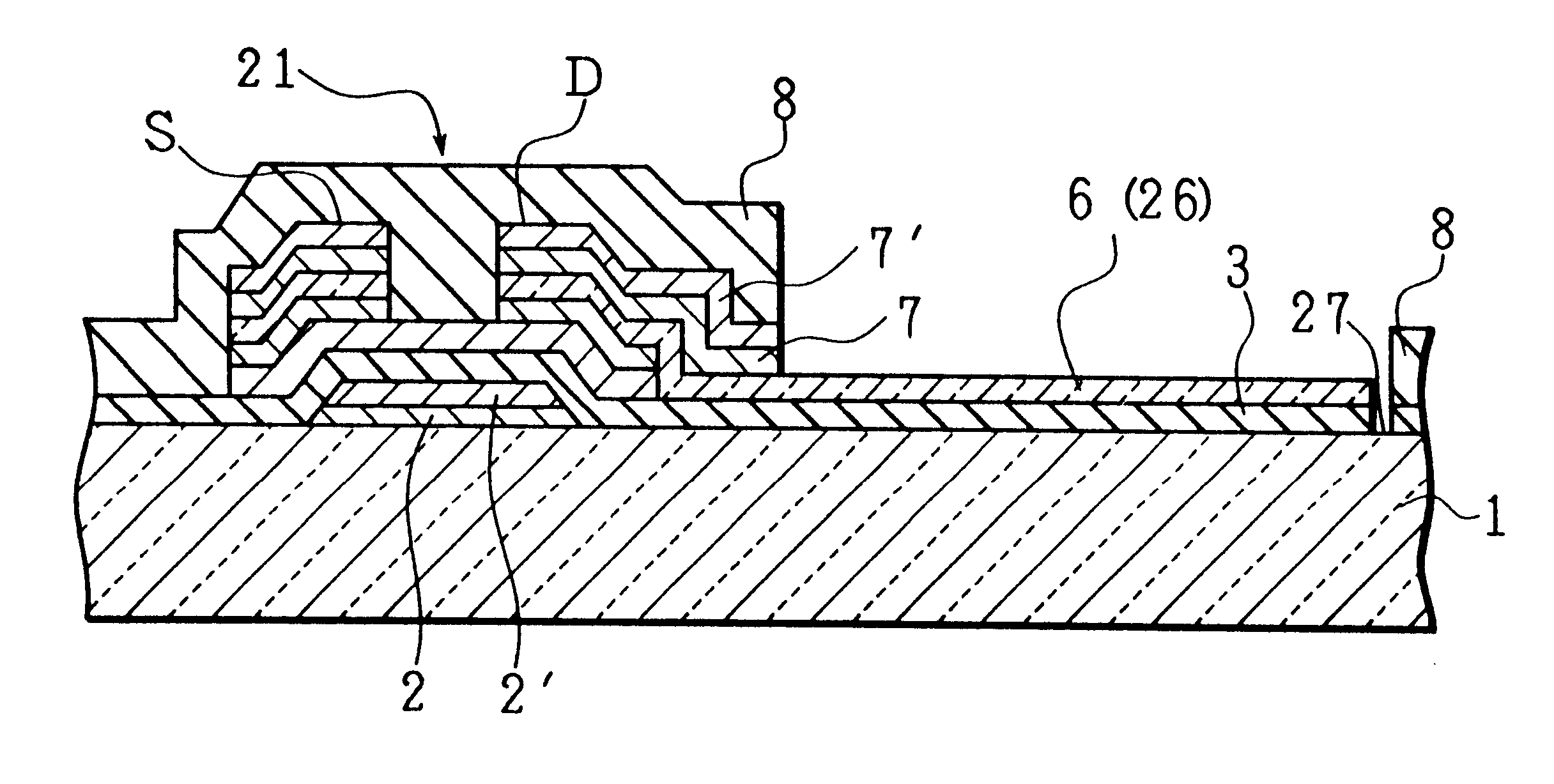
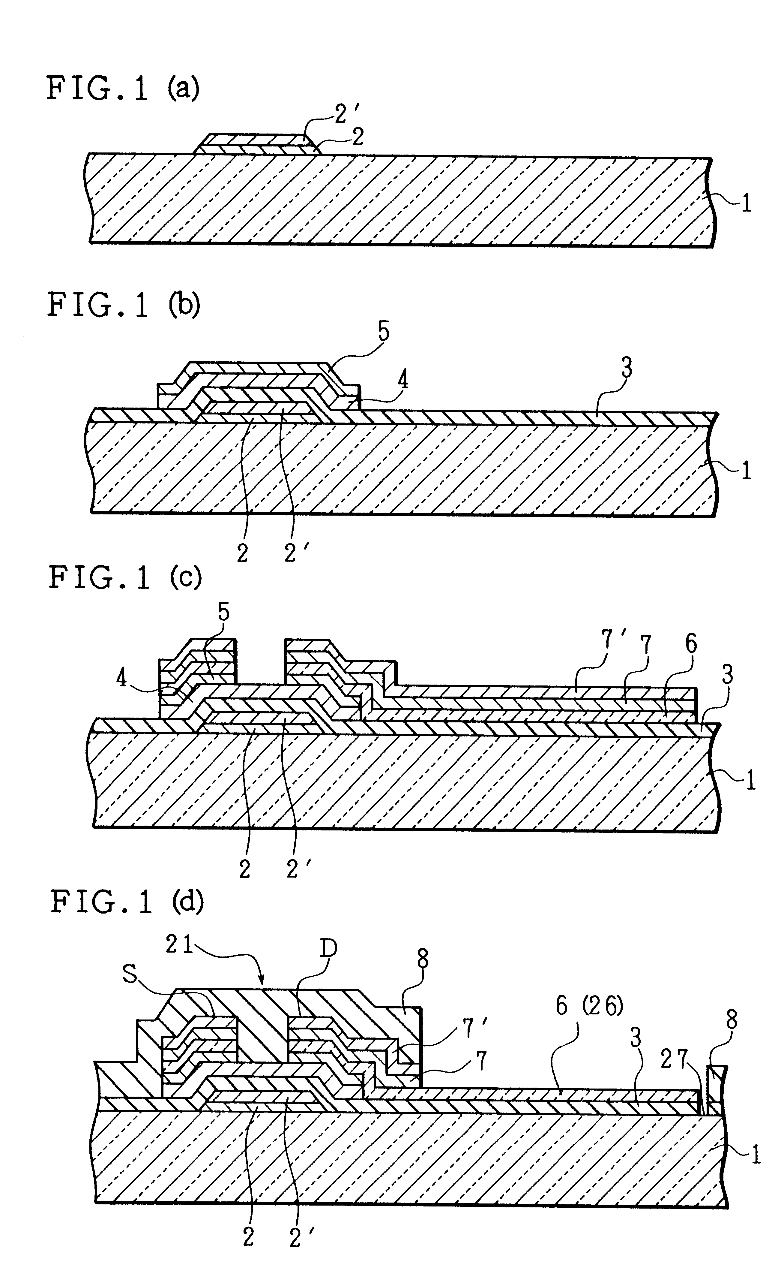
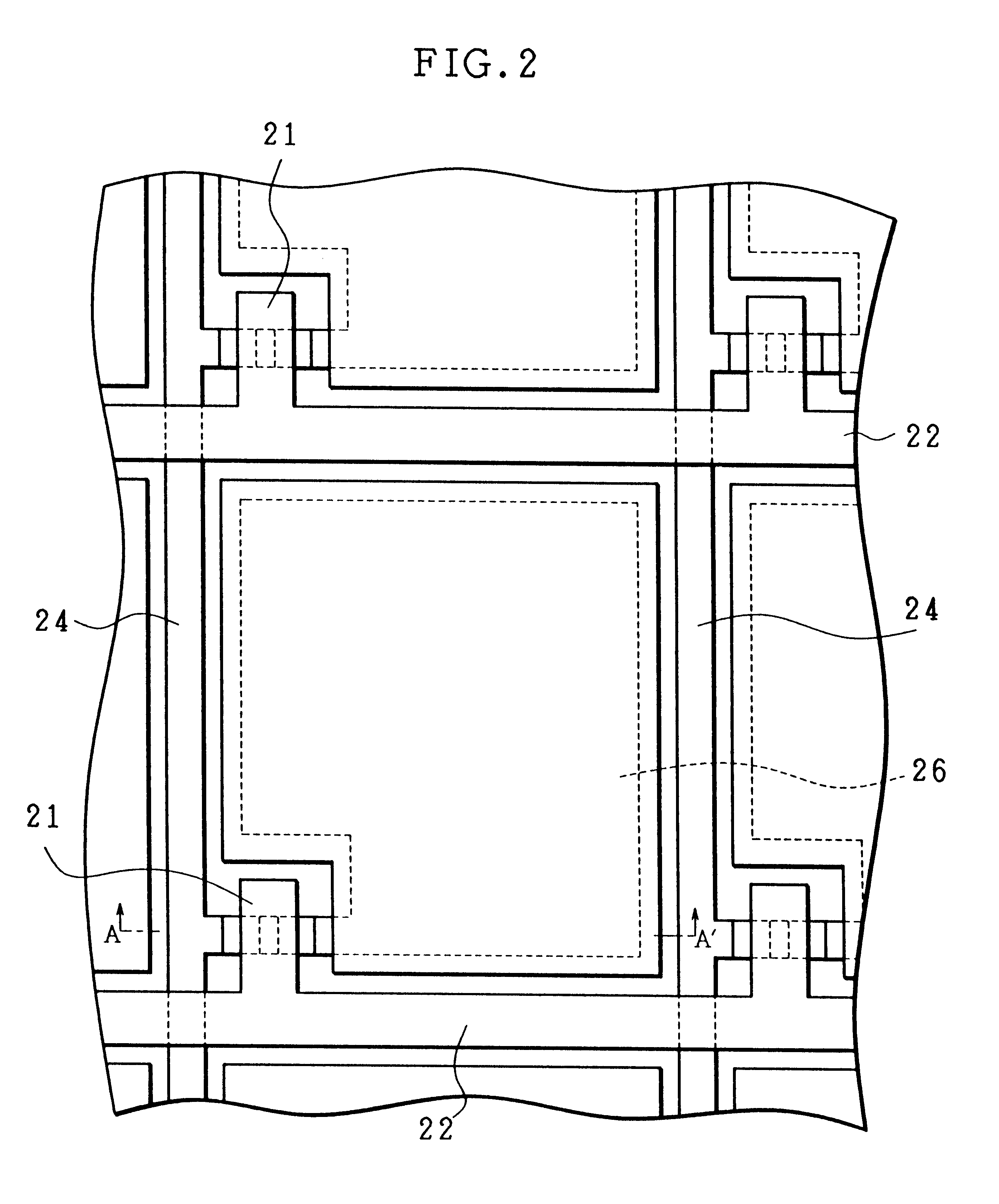
FIGS. 1(a) through 1(d) are cross sections taken on line A--A' in FIG. 2, explaining a manufacturing method of a liquid crystal display of the present embodiment. FIG. 2 is a plan view depicting a TFT array substrate forming the liquid crystal display of the present embodiment.

As shown in FIG. 2, the TFT array substrate of the present embodiment is provided with, on its main surface, a plurality of parallel gate signal lines 22 and a plurality of parallel source signal lines 24, which are aligned in such a manner so as to intersect with each other at right angles, thereby forming a matrix. More specifically, the gate signal lines 22 and source signal lines 24 are provided on the TFT array substrate through an insulating film 3 shown in FIG. 1 in such a manner so as to intersect with each other at right angles, and a pixel electrode 26 is provided at each intersection of the gate signal lines 22 and source signal lines 24. Further, a matrix of TFTs 21 are provided in one-to-one corre...

embodiment 2

The following will explain another embodiment of the manufacturing method of the TFT array substrate. Hereinafter, like components are labeled with like reference numerals with respect to Embodiment 1, and the description of these components is not repeated for ease of explanation.

FIG. 3 is a view explaining a forming method of the exposed portion of the external outlet electrode portion 23 of the gate signal line on the TFT array substrate in accordance with the manufacturing method of the liguid crystal display of the present embodiment. FIG. 4 is a view explaining a forming method of the exposed portion of the external outlet electrode portion 25 of the source signal line of the TFT array substrate in accordance with the manufacturing method of the liquid crystal display of the present embodiment.

The external outlet electrode portion 23 of the gate signal line is initially formed as the post-etching first metal film 2 and second metal film 2' in the first photo-etching process sh...


PUM


Abstract

A manufacturing method of a liquid crystal display of the present invention is a manufacturing method of a liquid crystal display having a glass substrate provided thereon with a matrix of thin film transistors, each having a semiconductor film pattern formed by photo-etching a high-resistance semiconductor film and a low-resistance semiconductor film, and a third metal film serving as a source metal film layer layered on the semiconductor film pattern, in which the semiconductor film pattern is formed on the glass substrate first, and thence the third metal film is layered on the glass substrate. Consequently, a liquid crystal display can be manufactured with a fewer number of manufacturing steps while at the same time the manufacturing costs can be saved by preventing a decrease in the yield caused by film separation.

Description

FIELD OF THE INVENTIONThe present invention relates to a method of manufacturing a liquid crystal display, and more particularly, to a method of manufacturing an active matrix type liquid crystal display in which a matrix of switching thin film transistors are formed in one-to-one correspondence with pixel portions.BACKGROUND OF THE INVENTIONGenerally, an active matrix type liquid crystal display is advantageous in many aspects, such as low power consumption, thinness, and lightness, and therefore, has been showing promise for use as a display device in diversified fields including a notebook personal computer, a mobile terminal, a TV set, etc.Under these circumstances, there has been an increasing need for an inexpensive active matrix type liquid crystal display. To this end, various techniques have been discussed to save the manufacturing costs by improving productivity of a thin film transistor (TFT) array substrate. Among others, a technique for reducing the number of times a ph...

Claims


Application Information

Patent Timeline
IPC IPC(8): G02F1/13G02F1/1362H01L21/70H01L21/84H01L27/12H01L21/336G02F1/1343G02F1/136G02F1/1368H01L21/77H01L29/786
CPCG02F1/13458G02F1/1362H01L27/1214H01L27/1288G02F1/1368H01L27/124
Inventor SHIMADA, YOSHINORI
Owner SHARP KK
Why Eureka
Try Eureka