Process for the production of an organic electroluminescent device

Inactive Publication Date: 2001-12-25
TDK CORPARATION
View PDF12 Cites 68 Cited by
  • Summary
  • Abstract
  • Description
  • Claims
  • Application Information

AI Technical Summary

Benefits of technology

The present invention provides an apparatus and a process for the production of an organic EL device, which permits a high freedom of apparatus designing, permits effective processing and gi

Problems solved by technology

There are many factors which are considered to deteriorate the device.
As a result, the light emission efficiency is caused to decrease, and a light-non-emitting area called a dark spot is caused to appear or a dark spot is caused to expand.
The surface thereof is often contaminated, and a cleaning step is therefore essential.
However, the above method has problems that the layer-forming chamber is required to share a space with the UV lamp and that the freedom of machine designing is decreased due to the location of the UV lamp.
Further, O.sub.3 is generated in the layer-forming chamber, and the above method is therefore not satisfactory with respe

Method used


Image

  • Process for the production of an organic electroluminescent device
  • Process for the production of an organic electroluminescent device

Examples


example 1

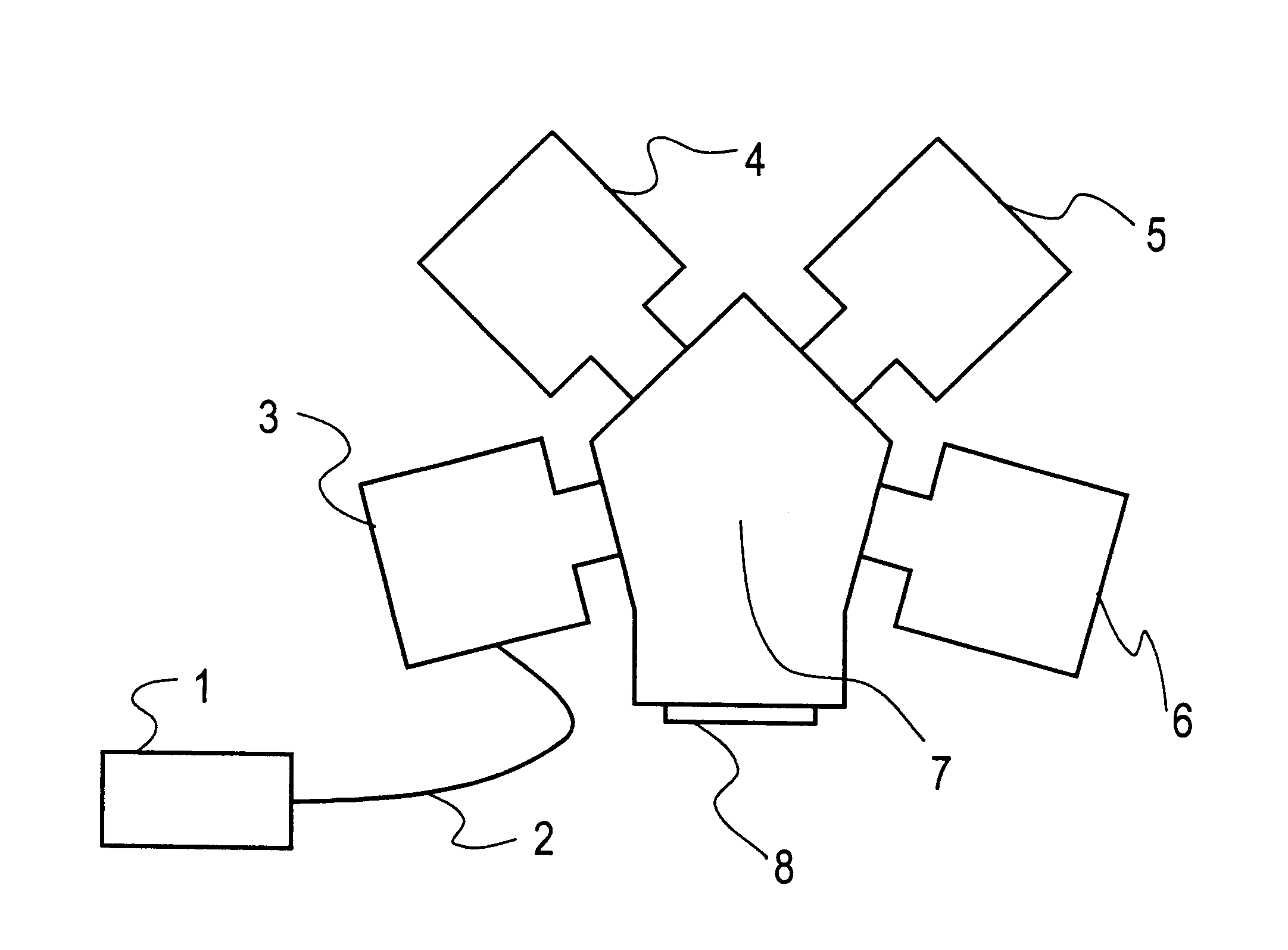
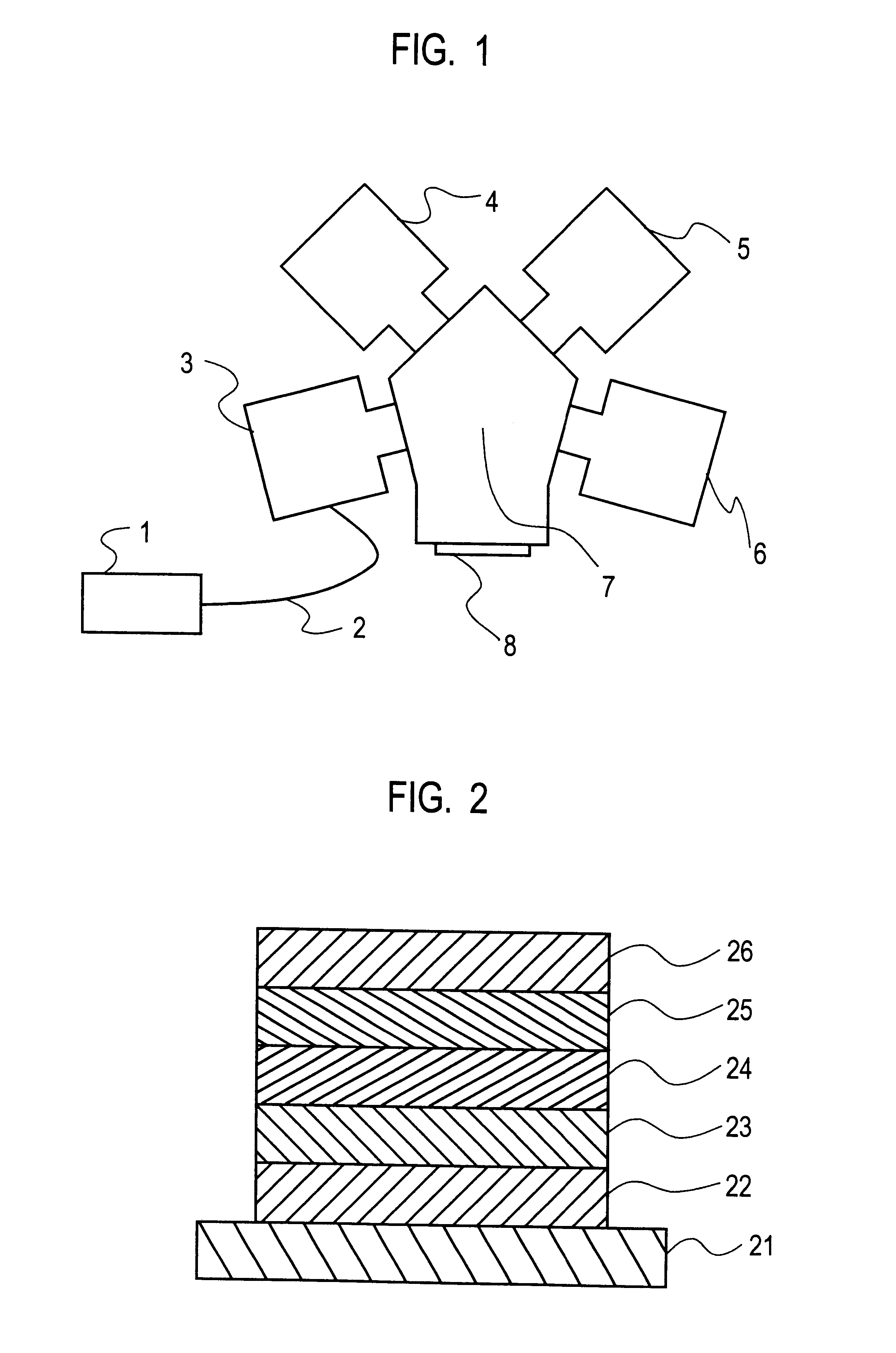
On a glass substrate, an ITO transparent electrode (hole-injecting electrode) was layer-formed and patterned so as to constitute pixels of 64 dots.times.7 lines (280.times.280 .mu.m per pixel) having a layer thickness of 85 nm. Then, the substrate having the patterned hole-injection electrode formed was ultrasonically washed with a neutral detergent, with acetone and with ethanol, and it was taken up from the boiling ethanol and dried. Then, the dry substrate was transported into a cleaning chamber, and the surface of the substrate was O.sub.3 -cleaned with an ozonizer for 5 minutes. In this case, O.sub.2 +N.sub.2 gases were used as feed gas, and the gas flow rates were 1 Nl / minute of O.sub.2 and 10 Ncc / minute of N.sub.2. The ozone gas which was generated had a concentration of 7 g / h. The atmospheric pressure in the cleaning chamber was 6.65.times.10.sup.3 Pa.

Then, the substrate was transferred from the cleaning chamber into a layer-forming chamber and fixed to a substrate holder of...

example 2

In Example 1, the cleaning with the ozonizer was replaced with cleaning with a UV lamp, and there was measured a time period required for obtaining a cleaning effect equivalent to that in Example 1, to show that the cleaning with the UV lamp required 30 minutes or more.


PUM

PropertyMeasurementUnit
Mass flow rateaaaaaaaaaa

Abstract

An apparatus and a process for the production of an organic EL device, which permits a high freedom of apparatus designing, permits effective processing and gives an organic EL device having a high light emission efficiency and excellent device characteristics, the apparatus comprising means of cleaning a surface of a substrate on which at least a hole-injecting electrode is formed, and means of forming an organic layer on the cleaned surface of the substrate, the cleaning means being for performing the cleaning with ozone gas generated with the ozonizer.

Description

The present invention relates to an organic EL device using an organic compound, and more specifically, it relates to an improvement of an interface between the hole-injecting electrode and the organic layer of an organic EL device.PRIOR ARTIn recent years, organic EL devices have been actively studied. Organic EL devices have a basic configuration structured by vaporizing a hole-transporting material such as triphenyldiamine (TPD) to form a thin film on a hole-injecting electrode, further laminating a light-emitting layer of a fluorescent material such as an aluminum quinol complex (Alq3) and further forming a metal electrode (electron-injecting electrode) having a low work function such as Mg. These organic EL devices are attracting attention due to their capability of a very high luminance of several 100 to several 10,000 cd / m.sup.2 at a voltage of about 10 V.It is considered that a material capable of injecting many holes into a light-emitting layer or a hole-injecting / transport...

Claims


Application Information

Patent Timeline
IPC IPC(8): C23C14/12C23C14/34H01L51/40H01L51/05H01L51/50H01L51/52H01L51/30H05B33/10H01L51/00H01L51/56H05B33/12H05B33/26
CPCC23C14/12C23C14/3414H01L51/001H01L51/5206H01L51/0059H01L51/0081H01L51/56H10K71/164H10K85/631H10K85/324H10K50/81H10K71/00
Inventor ARAI, MICHIONAKAYA, KENJI
Owner TDK CORPARATION
Why Eureka
Try Eureka