

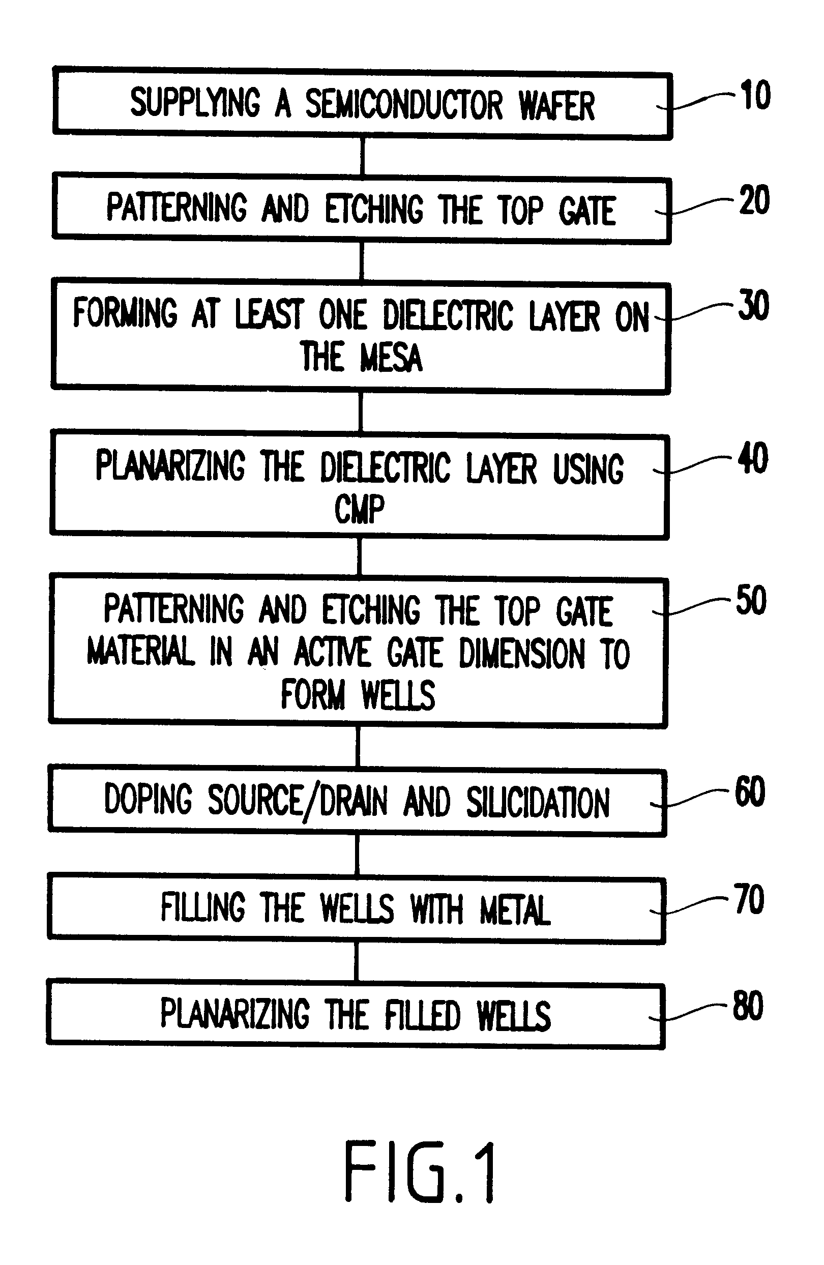
Two-step MOSFET gate formation for high-density devices
a technology of mosfet and gate, which is applied in the direction of semiconductor devices, electrical devices, transistors, etc., can solve the problems of inability to use materials, no advantages over conventional devices in source/drain resistance, and difficulty in lithography needed to produce small device features
- Summary
- Abstract
- Description
- Claims
- Application Information
AI Technical Summary
Benefits of technology
Problems solved by technology
Method used
Image

Examples
first embodiment
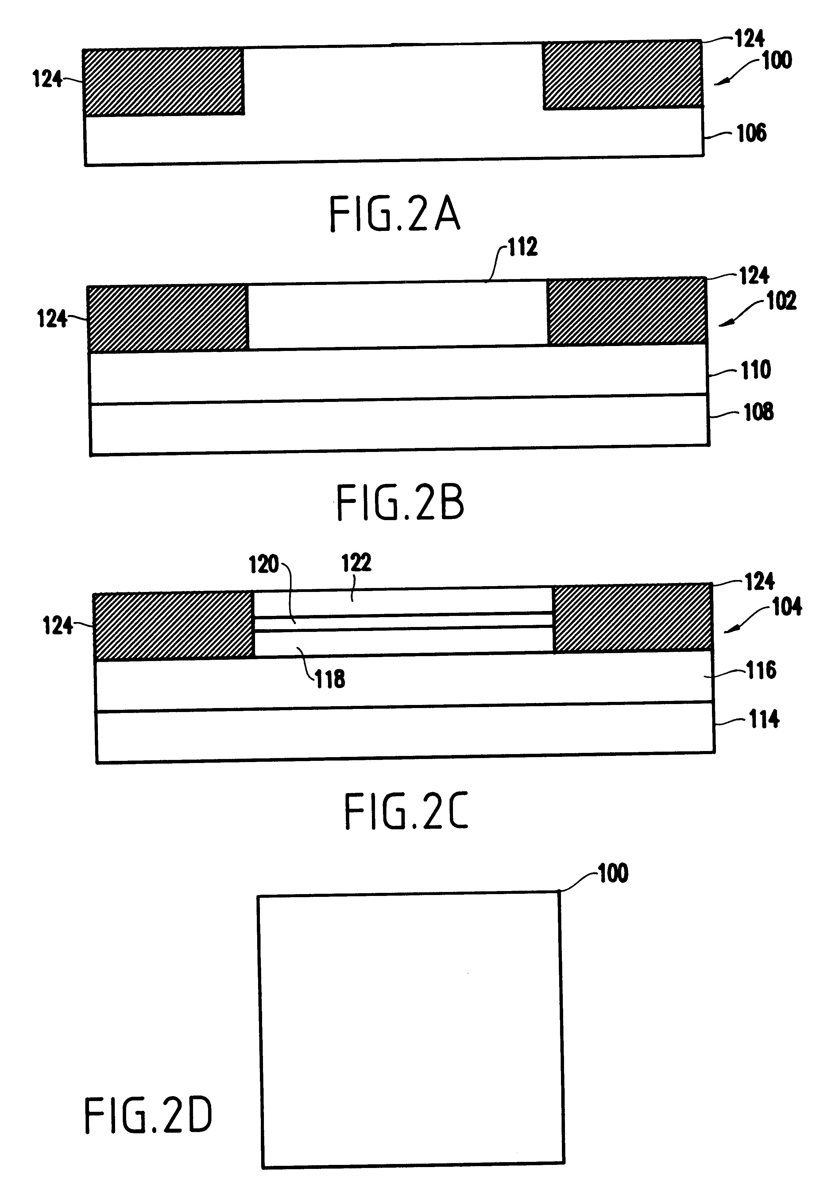
As alluded to above, the two-step gate definition method is relatively independent of the structure of the active semiconductor layers under the gate. The process can be used in many kinds of MOSFET devices. Possible starting wafers include bulk silicon wafer 100 (e.g., as shown in FIG. 2(a)), silicon on insulator (SOI) 102 (e.g., as shown in FIG. 2(b)) or more complex structures such as silicon wafer with a backgate 104 (e.g., as shown in FIG. 2(c)).
Referring now to FIGS. 3(a)-(c), for exemplary purposes, the substrate wafer starting material is a plain silicon wafer 100 with active areas defined by shallow trench isolation. Typical shallow trench isolation (STI) areas are formed by etching a trench of a few hundred nanometers in depth into the substrate, creating a thin barrier or isolation layer, filling the trench with a dielectric such as oxide somewhat thicker than the depth of the trench, then using CMP to planarize the deposited dielectric. A topgate mesa stack 125 is formed...
second embodiment
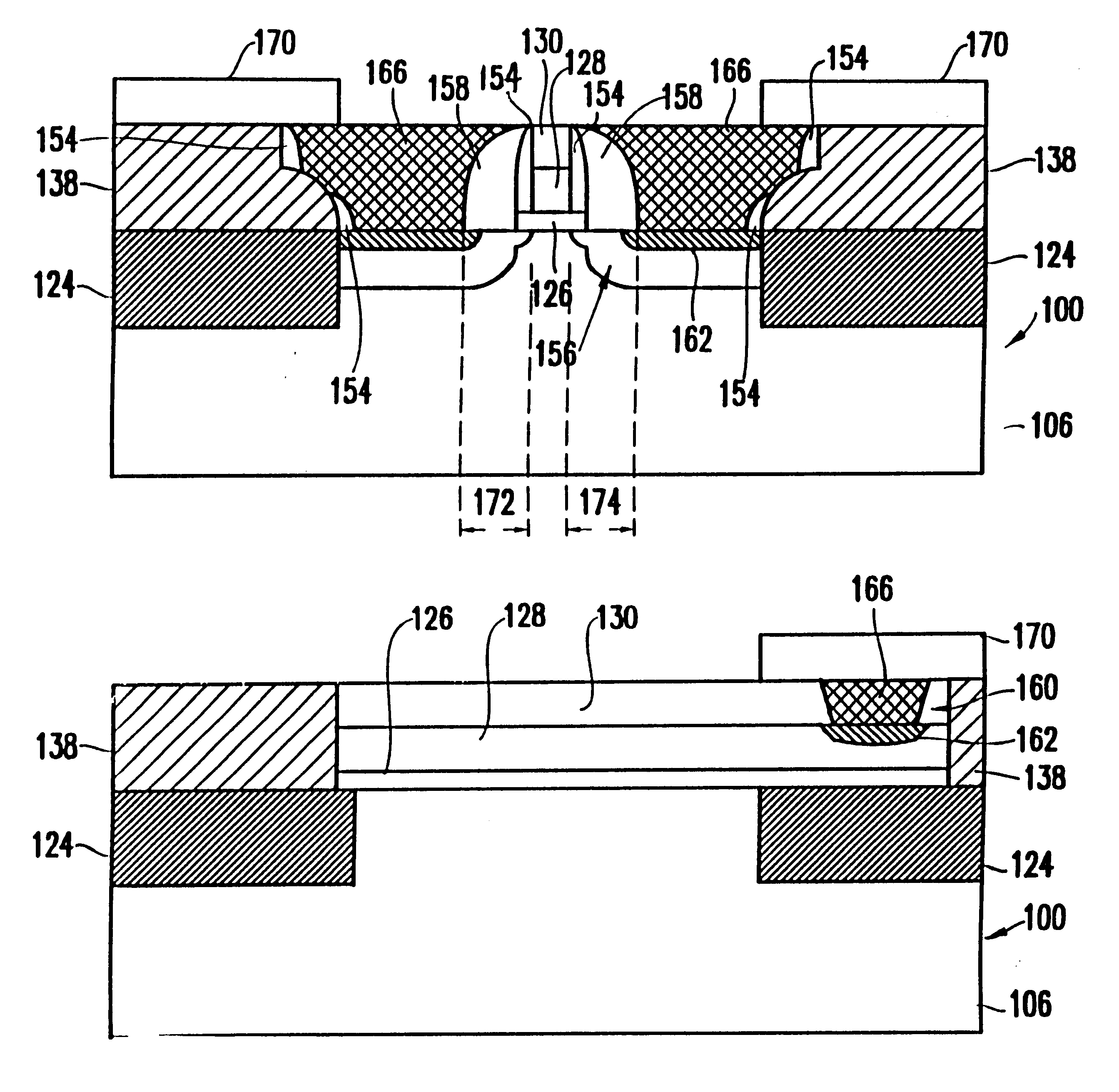
A second, further embodiment of the present invention includes an additional processing step. Referring now to FIG. 8, the source / drain wells with metal fill 166 (e.g., tungsten) are depicted. This may be done by depositing a blanket layer of CVD tungsten metal to fill the wells 144, 146 and then CMP processing back until the CMP stopping layers 130 are exposed. Alternatively, source / drain wells 144, 146 may be filled by electroplating. Gate contact 164 should also be filled at this time. Filling the gate contact 164 allows for returning the wafer surface 167 to a planar structure again following this CMP processing.
In either the first or second embodiment, metallization of the topgate may occur through the deposition of metal 170 (e.g., see FIG. 9). As illustrated, the overlay tolerance of metal 170 on the source / drain extension regions 156 can be quite relaxed, as the actual gate region is hidden from metal 170. This may be true even if the source / drain wells 144, 146 are shrunk q...
PUM
 Abstract
Description
Claims
Application Information