Build-up board package for semiconductor devices

a technology for semiconductor devices and build-up boards, which is applied in the manufacture of printed circuits, printed circuit parts, basic electric elements, etc., and can solve problems such as increased costs

Inactive Publication Date: 2002-01-22
SHINKO ELECTRIC IND CO LTD
View PDF7 Cites 19 Cited by
  • Summary
  • Abstract
  • Description
  • Claims
  • Application Information

AI Technical Summary

Problems solved by technology

However, there is a problem in that the process requires a large number of steps causing an increased cost when forming insulating layers on both sides of a core board 12 by application of a

Method used


Image

  • Build-up board package for semiconductor devices
  • Build-up board package for semiconductor devices
  • Build-up board package for semiconductor devices

Examples


example 2

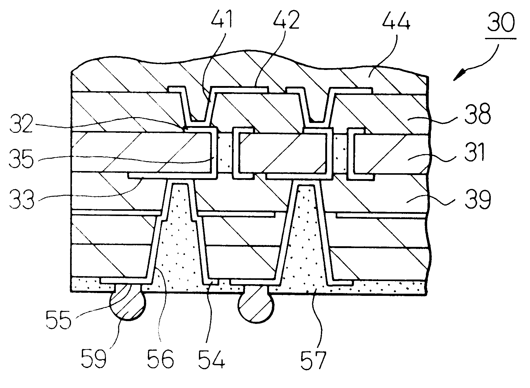
Another preferred embodiment of the package structure of the present invention will be described with reference to FIGS. 4A to 4C, in which the corresponding parts are denoted by the same symbols as used in FIG. 2.

As shown in FIG. 4A, insulating layers 38 and 39 are formed on a core board 31 and viaholes 40 are bored through the insulating layer 38. At this stage, no viaholes are formed in the insulating layer 39.

Electroless and the subsequent electrolytic copper plating treatments are conducted to form a copper plated coating on the insulating layer 38, the side wall of the viaholes 40 and the insulating layer 39.

The copper plated coatings on the insulating layers 38 and 39 are patterned by etching to form a wiring pattern 42 and a flat conductor layer 60.

A laminate of upper wiring patterns with intervening insulating layers is formed on the front side of the board 31.

Insulating layers 45 and 46 are formed on the flat copper plated coating 60 on the back side of the board 31.

Referr...


PUM


Abstract

A package for semiconductor devices, comprising a core board having a front side with a front side base wiring pattern formed thereon and a back side with a back side base wiring pattern formed thereon, the front and back side wiring patterns being electrically connected to each other through a conductor segment penetrating the core board; a front side laminate of upper wiring patterns with intermediate insulating layers intervening therebetween on the front side base wiring pattern, in which each adjacent pair of the upper wiring patterns are electrically connected to each other through a via plated coating on a side wall of viaholes penetrating one of the intermediate insulating layers that intervenes between the adjacent pair and in which an outermost one of the upper wiring patterns is patterned for electrical connection to a semiconductor chip; a back side laminate of insulating layers on the back side base wiring pattern; an external connection wiring pattern including external connection terminals on the back side laminate of insulating layers; wherein the external connection wiring pattern is electrically connected to the back side base wiring pattern through a via penetrating the back side laminate of insulating layers.

Description

1. Field of the InventionThe present invention relates to a package for semiconductor devices.2. Description of the Related ArtIt is a growing trend to use a package for semiconductor devices in the form of a build-up board composed of a core board having multilayer wiring patterns formed on both sides by build-up process.FIG. 1 shows a build-up board 10 having a core board 12 of an insulating material having base wiring patterns 13 and 14 formed on both sides and electrically connected to each other by a throughhole plated coating 15.Insulating layers 16 and 17 are formed on the base wiring patterns 13 and 14, respectively, and contain viaholes 16a and 17a.Electroless and the subsequent electrolytic plating treatments are conducted to form a copper plated coating on the insulating layers 16 and 17 and the side walls of the viaholes 16a and 17a. The copper plated coating is then patterned by etching to form upper wiring patterns 18 and 19, as a first layer, which are connected to th...

Claims


Application Information

Patent Timeline
IPC IPC(8): H01L23/498H01L23/48H05K1/11H05K3/46H01L23/12
CPCH01L23/49827H01L2224/16H01L2924/01078H01L2924/15174H01L2924/15311H01L2924/15312H05K1/114H05K3/4602H05K2201/0195H05K2201/09509H05K2201/09518H05K2201/09845H05K2201/10734H01L2224/73204H01L2224/16225H01L2224/32225H01L2924/00
Inventor IIJIMA, TAKAHIROROKUGAWA, AKIO
Owner SHINKO ELECTRIC IND CO LTD
Why Eureka
Try Eureka