Liquid crystal display device using thin-film transistor and method for manufacturing the same

Inactive Publication Date: 2006-09-21
SHARP KK
View PDF6 Cites 6 Cited by
  • Summary
  • Abstract
  • Description
  • Claims
  • Application Information

AI Technical Summary

Benefits of technology

[0019] Further, the thin-film transistor (TFT) array and the method for manufacturing the same have not been known in the pas

Problems solved by technology

However, for preparing the thin films and for patterning, expensive and low-throughput vacuum systems with complicated structure such as sputtering system, CVD system and etching system must be used.
This makes the manufacturing process more complicated and requires higher manufacturing cost.
However, many production processes are still required, and it is not possible to manufacture the thin-film transistors at low cost and with high throughput.
However,

Method used


Image

  • Liquid crystal display device using thin-film transistor and method for manufacturing the same
  • Liquid crystal display device using thin-film transistor and method for manufacturing the same
  • Liquid crystal display device using thin-film transistor and method for manufacturing the same

Examples


embodiment 1

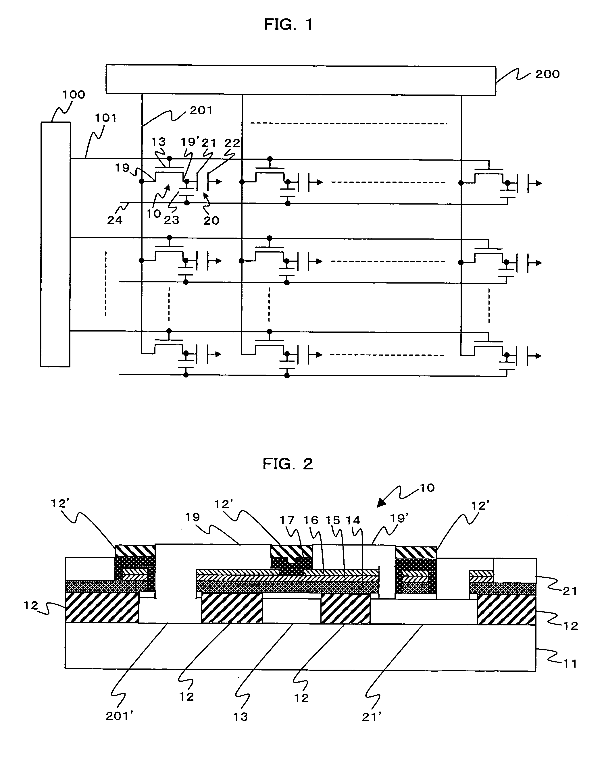
[0036]FIG. 1 is a schematical diagram of a liquid crystal display device of active matrix type using a thin-film transistor according to the present invention. To match scan lines 101 as selected by a scan line driving circuit 100, data (voltage) is supplied to a thin-film transistor 10 from a data line driving circuit 200 via data lines 201.

[0037] The thin-film transistor 10 is provided at an intersection of the scan line 101 and the data line 201. The scan line 101 is connected to a gate electrode 13 of the thin-film transistor 10. The data line 201 is connected to a source electrode 19 of the thin-film transistor 10.

[0038] A drain electrode 19′ of the thin-film transistor 10 is connected to a pixel electrode 21 of a liquid crystal element 20. The liquid crystal element 20 is positioned between the pixel electrode 21 and a common electrode 22, and it is driven by data (voltage) supplied to the pixel electrode 21. An auxiliary capacity 23 to temporarily maintain the data (voltage...

embodiment 2

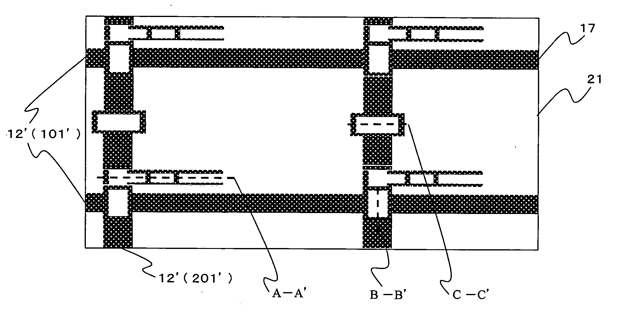
[0055]FIG. 8 is a cross-sectional view of the thin-film transistor 10 shown in FIG. 1. It is different from the cross-sectional view of the thin-film transistor 10 of FIG. 2 in the arrangement of the ohmic contact layer (n+ semiconductor layer) 16 and the protective layer 17. Description will be given below on the processes for manufacturing this thin-film transistor. The gate-source line process is the same as the process shown in FIG. 3. The next process for preparing the thin-film transistor is shown in FIG. 9.

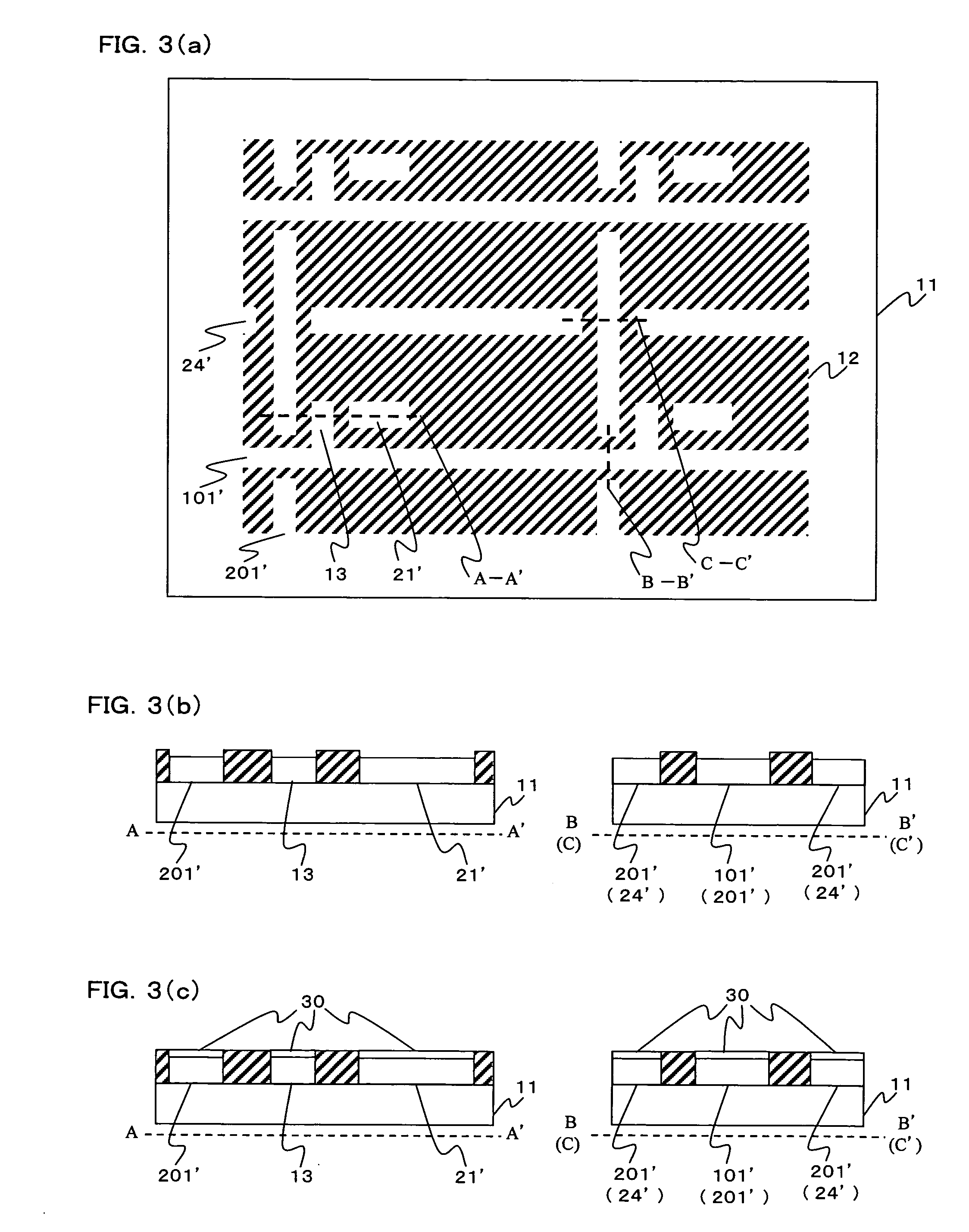
[0056]FIG. 9 represents drawings to show processes for preparing the thin-film transistor subsequent to the gate-source line process shown in FIG. 3. As shown in FIG. 9 (a), a gate insulator 14, an a-Si semiconductor film 15 and a protective film 17 are sequentially formed. FIG. 9 (c) represents a cross-sectional view of the thin-film transistor 40 along the broken line A-A′, the line crossing portion 41 along the broken lines B-B′ and the broken line C-C′.

[0057] Next, si...

embodiment 3

[0062]FIG. 13 is a cross-sectional view of a thin-film transistor 10 shown in FIG. 1. This is different from the cross-sectional view of the thin-film transistor of FIG. 8 in that the second light transmission type photosensitive resin 12′ is not used. Description will be given below on the process for manufacturing the thin-film transistor. The gate-source line process is the same as the process shown in FIG. 3. The subsequent process for preparing the thin-film transistor is the same as the processes shown in FIG. 9, FIG. 10, and FIG. 11 (b). FIG. 14 shows the processes subsequent to the processes shown in FIG. 11 (b).

[0063] The arrangement shown in FIG. 14 is different from the arrangement of FIG. 11 (c) and FIG. 11 (d) in that the cap metal 30 is processed by etching as shown in FIG. 14 (a), and the second light transmission type photosensitive resin 12′ and the resist 110 are removed off as shown in FIG. 14 (b).

[0064]FIG. 15 represents processes for preparing the thin-film tr...


PUM


Abstract

The present invention provides a liquid crystal display device using a thin-film transistor, and the invention also provides a method for manufacturing the liquid crystal display device.
In openings of a first light transmission type photosensitive resin formed on an insulating substrate, a gate electrode, a source line, and a pixel contact layer are prepared. On these components, a gate insulator, a semiconductor layer, an ohmic contact layer (n+ semiconductor layer) and a protective film are prepared. Further, in openings of a second light transmission type photosensitive resin, a source electrode, a drain electrode, and a pixel electrode are prepared. Also, the crossing portion connecting line formed at the opening of the second light transmission type photosensitive resin is, similarly to the source line or the gate line, made of baked silver produced by baking an ink containing silver fine particles plotted by ink jet process. This makes it possible to simplify the production process and to prevent the increase of wiring resistance of the source line and gate line.

Description

FIELD OF THE INVENTION [0001] The present invention relates to a liquid crystal display device using a thin-film transistor with a gate electrode, a source electrode, and a drain electrode prepared by ink jet plotting. The invention also relates to a method for manufacturing the same. BACKGROUND OF THE INVENTION [0002] A thin-film transistor (TFT) used in a liquid crystal display device of active matrix type comprises a gate electrode with metal film such as chromium, a gate insulator film made of SiNx, a semiconductor layer made of amorphous silicon, an ohmic contact layer doped with impurities such as phosphor, a source electrode and a drain electrode made of metal film such as chromium, and a protective film laminated in this order on a substrate. [0003] The thin-film transistor as given above is produced by preparing a multiple of thin films on a glass substrate and by performing photo-lithographic process on the thin films. However, for preparing the thin films and for patterni...

Claims


Application Information

Patent Timeline
IPC IPC(8): G09G3/36H01J1/62
CPCG02F1/136286G02F2001/136295H01L27/1292H01L27/1285H01L27/1288H01L27/124G02F1/136295B26B19/044B26B19/06
Inventor YOSHIMOTO, YOSHIKAZU
Owner SHARP KK
Why Eureka
Try Eureka