Three-dimensional packaging technology for multi-layered integrated circuits

a technology of integrated circuits and packaging, applied in the field of three-dimensional packaging, can solve the problems of high manufacturing cost, complex interconnection schemes, and limit the number of ic chips which can be stacked vertically

Inactive Publication Date: 2002-03-12
REVEO
View PDF17 Cites 220 Cited by
  • Summary
  • Abstract
  • Description
  • Claims
  • Application Information

AI Technical Summary

Benefits of technology

Accordingly, a primary object of the present invention is to provide an improved method and apparatus for packaging multi-layered integrated circuits in a way which avoids the shortcomings and drawbacks of prior art technologies.

Problems solved by technology

Clearly, there is much wasted space using such an arrangement that an opportunity is presented to explore newer more space-efficient packaging concepts for IC chips.
While these prior art 3-D packaging approaches have been shown to work, they have many shortcomings and drawbacks, including: limitations on the number of IC chips which can be stacked vertically; very high manufacturing costs; and complex interconnection schemes.
Texas Instruments (TI) and Thompson are using a stacked tape-automated bonding (TAB) approach which has significant limitations in that the number of vertically-stacked chip layers is 20 or less.
Irvine Sensors Corporation (ISC) is pursing an approach that is more promising, although it too suffers from the following limitations: the number of layers of IC chips that can be stacked is limited to less than 100 because of alignment difficulties inherent in the manufacturing method; the number of layers which can be interconnected is limited unless each chip is individually personalized, a step that increases cost dramatically; the edge wiring density is low due to inaccurate alignment between the vertically disposed chips; the low yield and high cost because tested chips must have sizes with narrow tolerances to achieve certain alignment accuracy; the manufacturing process is too costly as the number of layers approaches 100; thermal and mechanical consideration add to manufacturing difficulties (i.e. heat must be carried to the edge of the stack for removal of IC chip layers and on an interchip bonding layer must be provided between to avoid delamination due to thermal mismatch); and the lack of flexibility in stack size.
However, this packaging technique suffers from numerous shortcomings and drawbacks which prevent it from being widely used in commercial practice.

Method used


Image

  • Three-dimensional packaging technology for multi-layered integrated circuits
  • Three-dimensional packaging technology for multi-layered integrated circuits
  • Three-dimensional packaging technology for multi-layered integrated circuits

Examples


Embodiment Construction

Referring now to the figures in the accompanying drawings, the illustrative embodiments of the present invention will be described in detail, wherein like elements will be indicated in figures with like reference numerals.

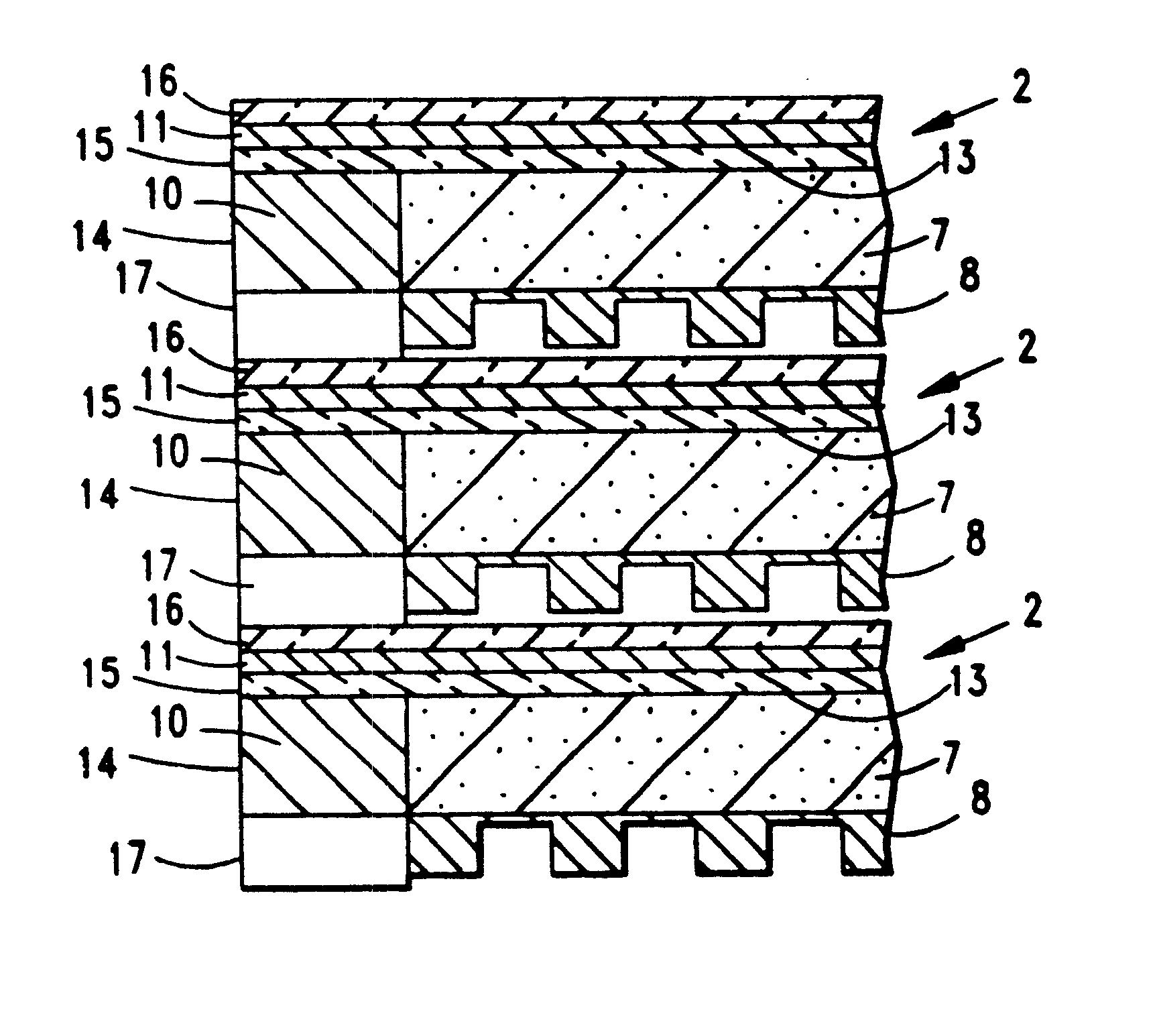
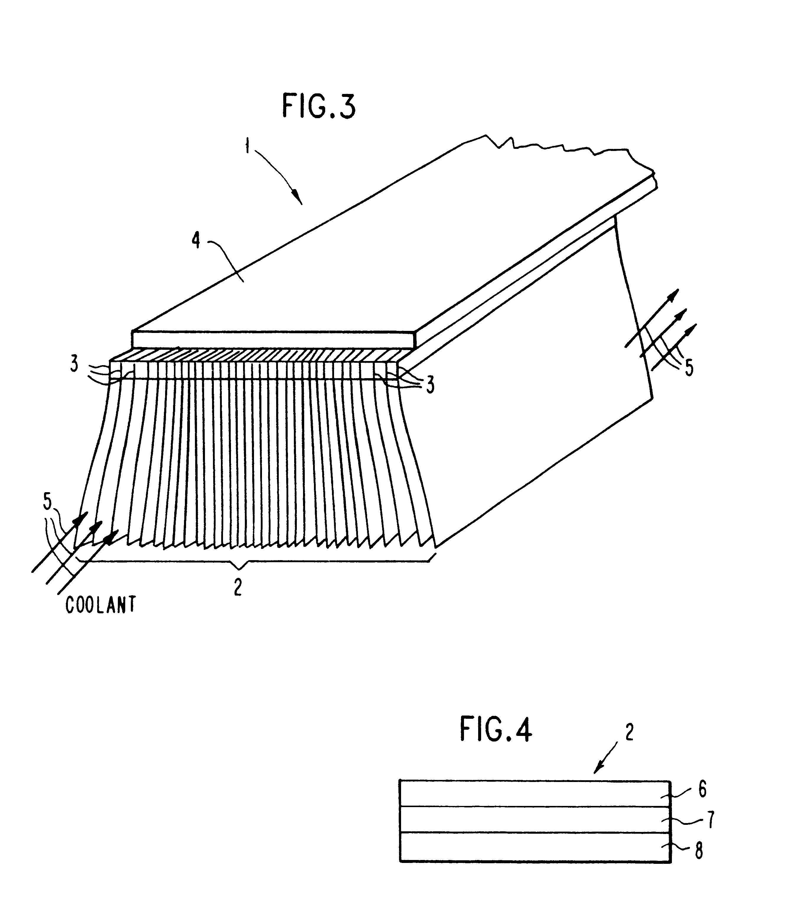
In FIG. 3, a perspective view of a Massive Fillo-leaf Technology (MFT) module according to the present invention is schematically illustrated. As shown, the MFT module 1 comprises a plurality of elements, i.e. integrated circuit (IC) layers, hereinafter referred to as "fillo-leaf" circuit layers 2, which are bonded together at their edges 3 so that the fillo-leaf circuit layers 2 extend in a cantilevered fashion from bonded edges 3. Each fillo-leaf circuit layer 2 supports a plurality of pairs of electrically or light conductive lines (not shown in FIG. 3) which extend from a common plane of bonded edges 3 to one or more comparators or other means (not shown in FIG. 3) forming a portion of the Massive IC Chip Selection Architecture (MSA) of the present invention. A...


PUM


Abstract

Disclosed is method and apparatus for packaging multilayered integrated circuit (IC) chips, on which logic circuits and/or memory arrays are disposed and interconnected in a novel way permitting the addressing (i.e. selection) of the logic circuits and/or arrays on these IC chip layers using a minimum number of connections and with the shortest propagation delays.

Description

BACKGROUND OF INVENTION1. Technical FieldThe present invention relates generally to a three-dimensional package for massive layers of integrated circuit (IC) chips, on which logic circuits and / or memory arrays are disposed and interconnected in a novel way to permit addressing (i.e. selection) of the circuits and / or arrays on these circuit layers using a minimum number of connections and with the shortest propagation delays.2. Brief Description of Prior ArtToday, most electronic packages are largely two-dimensional in arrangement. Typically, multiple chips are placed on a single planar module called a Multiple Chip Module (MCM). These modules are coarse in granularity, with feature sizes of 5 to 10 mils. Because of this coarse granularity, many metallization levels are required to wire the module. Typically, this category of IC packaging involves twenty to forty levels of metallization.To reduce the number of metal layers, and thereby improve performance, newer 2-D modules use finer...

Claims


Application Information

Patent Timeline
Patent Type & Authority Patents(United States)
IPC IPC(8): H01L23/367H01L23/52H01L23/34H01L23/538H01L25/065H01L23/473
CPCH01L23/3672H01L23/5387H01L25/0652H01L23/473H01L2924/0002H01L2225/06551H01L2924/00
Inventor FARIS, SADEG M.
Owner REVEO
Why Eureka
Try Eureka