Method for increasing a very-large-scale-integrated (VLSI) capacitor size on bulk silicon and silicon-on-insulator (SOI) wafers and structure formed thereby

a technology of silicon-on-insulator and capacitor, which is applied in the direction of capacitors, semiconductor devices, electrical equipment, etc., can solve the problems of difficult to implement a large capacitor in a chip, the process of making deep silicon island capacitors is very expensive, and the "real estate" of the chip is already very limited

Inactive Publication Date: 2002-03-19
GLOBALFOUNDRIES INC
View PDF14 Cites 99 Cited by
  • Summary
  • Abstract
  • Description
  • Claims
  • Application Information

AI Technical Summary

Benefits of technology

Another object is to provide a method of forming a low-cost capacitor, without any additional processing costs.
Yet another object is to use a phase-shift mask technique to increase the capacitor density to reduce pitch by patterning the sub-lithographic feature by intentionally increasing the ratio of silicon width to spacing between adjacent islands.
With the unique and unobvious features of the invention, a low cost method is provided to form a high performance capacitor. Further, the present invention is useful for both bulk and SOI substrates. Additionally, the technique is especially useful for SOI substrates with a thick silicon layer (e.g., having a thickness greater than 0.5 .mu.m).
Another advantage of the invention is that large capacitors are built simultaneously with a high performance transistor or a transistor with a wrap-around gate structure.

Problems solved by technology

However, it is very difficult to implement a large capacitor in a chip where the chip "real estate" is already very limited.
This process of making deep silicon island capacitors is very expensive, unless DRAM array is built on the same chip.
However, for other chips such as SOI, or silicon-on-oxide, due to the existing buried oxide layer, if the only goal is to make a large capacitor using a deep silicon island structure, the processing and other costs will be prohibitive and thus impractical.
This also increases the cost of processing significantly.
However, this technique makes planarization and interconnection more difficult.
Thus, this approach also is not a good option in making a large capacitor.
Other methods, such as a "roughened surface" capacitor, etc. are equally impractical and require special techniques to implement.
This technique also increases the surface (and thus capacitance) of the structure.
However, as mentioned above, such techniques are impractical and are not easily implemented.
Further, the capacitance enhancement is not reproducible, and therefore not suitable especially for some analog applications where the capacitor size must be precisely controlled.
Thus, a problem arises regarding how to build large capacitors with good area control (e.g., providing a specific capacitance) on a chip, without extra process cost.

Method used


Image

  • Method for increasing a very-large-scale-integrated (VLSI) capacitor size on bulk silicon and silicon-on-insulator (SOI) wafers and structure formed thereby
  • Method for increasing a very-large-scale-integrated (VLSI) capacitor size on bulk silicon and silicon-on-insulator (SOI) wafers and structure formed thereby
  • Method for increasing a very-large-scale-integrated (VLSI) capacitor size on bulk silicon and silicon-on-insulator (SOI) wafers and structure formed thereby

Examples


Embodiment Construction

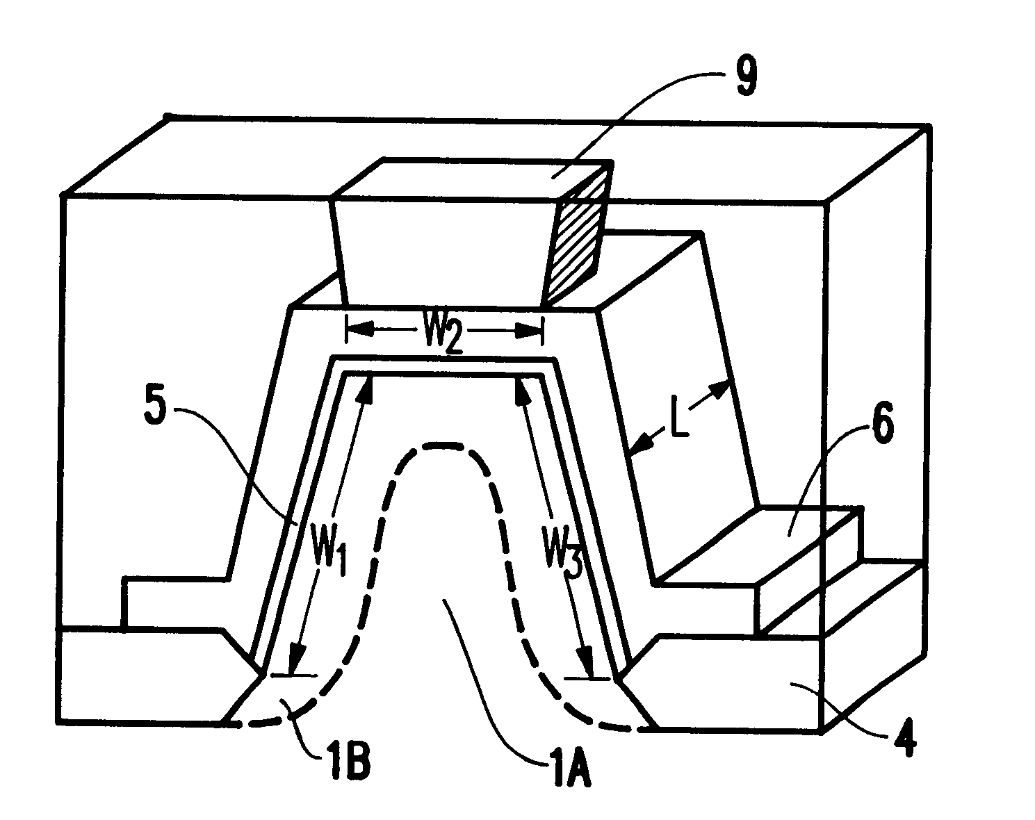
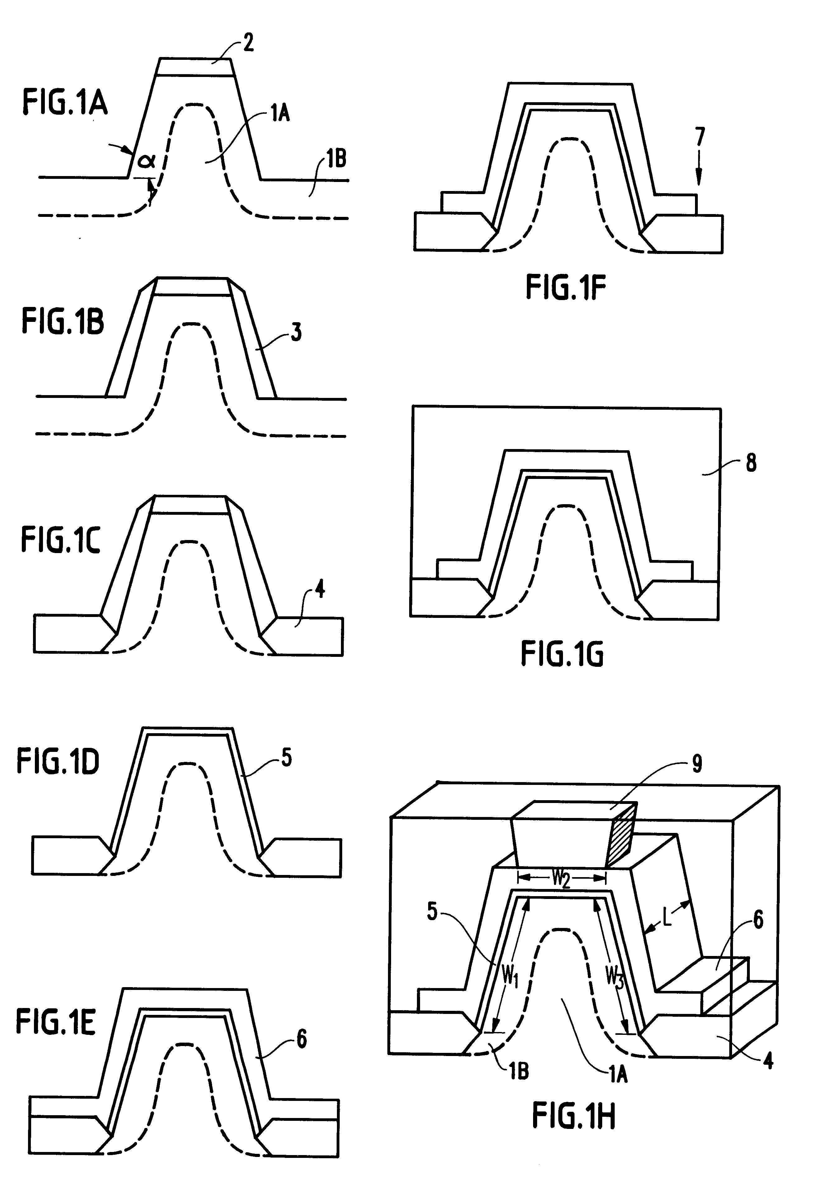
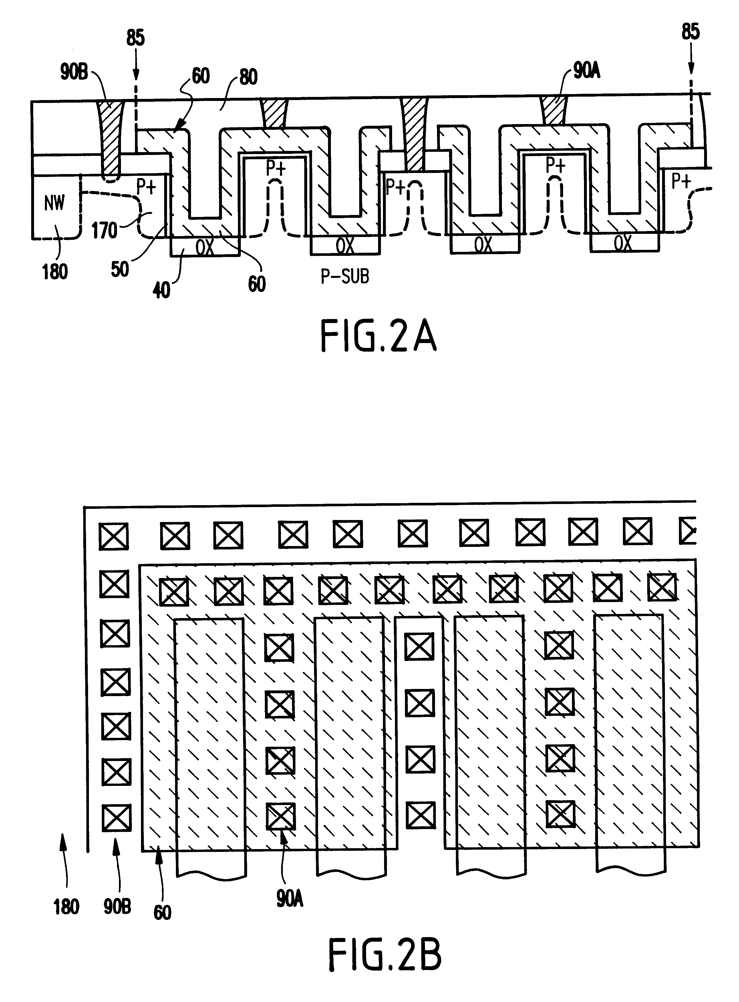
Referring now to the drawings, and more particularly to FIGS. 1-5, there are shown preferred embodiments of the method and structures according to the present invention.

Generally, the invention is a method for forming a semiconductor device by forming at least one silicon island on a bulk silicon wafer or a silicon-on-insulator (SOI) wafer. In the exemplary process below, a capacitor is formed. The SOI wafers mentioned here have a relatively thicker silicon thickness (e.g., greater than about 5000 .ANG. silicon thickness). The insulation layer is in the range of about 800 .ANG. to about 3000 .ANG., depending upon whether the SOI substrate is formed by a wafer bonding technique or by a SIMOX process. It is noted that the insulation layer is preferably as thin as possible. However, if the insulation is too thin, then an oxide breakdown may occur and the device may become "leaky". If the insulation is too thick, then a thermal penalty of the device will result.

The wafer bonding typical...


PUM

PropertyMeasurementUnit
dielectric constantaaaaaaaaaa
thicknessaaaaaaaaaa

Abstract

A method of forming a semiconductor device, includes forming at least one conductive island having a predetermined sidewall angle in a conductive substrate, forming a dielectric material over the at least one island, forming a conductive material over the dielectric material, and forming a contact to the conductive material and the at least one island.

Description

1. Field of the InventionThe present invention generally relates to a method of forming a semiconductor device, and more particularly to a method for increasing a capacitor size on bulk and silicon-on-insulator (SOI) wafers.2. Description of the Related ArtLarge capacitors are usually needed for integrated circuits such as decoupling capacitors for a power or signal bus stabilization, or capacitors for analog application circuits such as reservoirs for a charge pump. However, it is very difficult to implement a large capacitor in a chip where the chip "real estate" is already very limited.Therefore, many methods have been proposed to increase the capacitor value without increasing the chip area. A first method is to form a deep silicon island capacitor. Making an array of deep silicon island capacitors where the capacitors are similar to those used in the DRAM used for cell node data storage. This process of making deep silicon island capacitors is very expensive, unless DRAM array ...

Claims


Application Information

Patent Timeline
Patent Type & Authority Patents(United States)
IPC IPC(8): H01L21/02H01L21/334H01L29/66H01L27/12H01L27/08H01L29/94H01L29/78
CPCH01L27/0805H01L27/1203H01L29/945H01L29/66181H01L28/90Y10S438/948Y10S438/947Y10S257/905H01L29/78
Inventor HSU, LOUIS L.WANG, LI-KONG
Owner GLOBALFOUNDRIES INC
Why Eureka
Try Eureka