Method for controlling photoresist baking processes

a technology of photoresist and baking process, which is applied in the direction of photomechanical treatment, electrical equipment, instruments, etc., can solve the problems that certain photoresist materials do not complete the transition from being soluble to being insoluble, and it is more difficult to strip off the photoresis

Inactive Publication Date: 2002-03-26
GLOBALFOUNDRIES INC
View PDF5 Cites 15 Cited by
  • Summary
  • Abstract
  • Description
  • Claims
  • Application Information

AI Technical Summary

Problems solved by technology

Certain photoresist materials do not complete the transition from being soluble to being insoluble in the developer based solely on the exposure to light.
As the photoresist material becomes more resistant to the etching process, however, it makes stripping off the photoresist more difficult to achieve.

Method used


Image

  • Method for controlling photoresist baking processes
  • Method for controlling photoresist baking processes
  • Method for controlling photoresist baking processes

Examples


Embodiment Construction

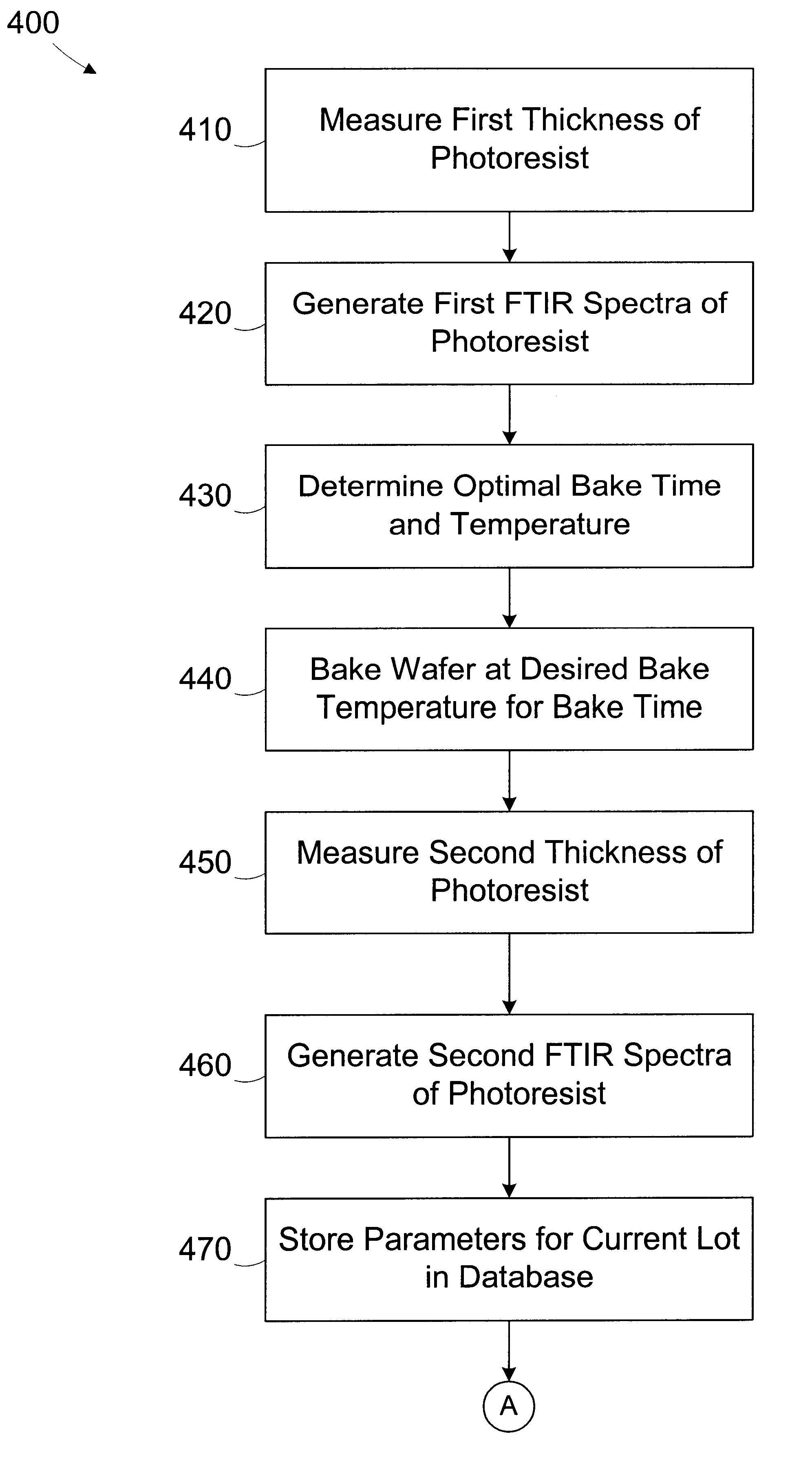
Illustrative embodiments of the invention are described below. In the interest of clarity, not all features of an actual implementation are described in this specification. It will of course be appreciated that in the development of any such actual embodiment, numerous implementation-specific decisions must be made to achieve the developers' specific goals, such as compliance with system-related and business-related constraints, which will vary from one implementation to another. Moreover, it will be appreciated that such a development effort might be complex and time-consuming, but would nevertheless be a routine undertaking for those of ordinary skill in the art having the benefit of this disclosure.

Turning now to the drawings, and, specifically referring to FIG. 2, a simplified block diagram of a processing line 200 for performing photolithography patterning of a wafer 205 is provided. The processing line 200 includes a stepper 210 that exposes the photoresist layer on the wafer ...


PUM

PropertyMeasurementUnit
timeaaaaaaaaaa
thicknessaaaaaaaaaa
) spectraaaaaaaaaaa

Abstract

A method and apparatus for controlling photoresist baking processes. A wafer is provided with the wafer having a layer of photoresist thereon. A first thickness of the photoresist layer is measured, and a first fourier transform infrared (FTIR) spectra of the photoresist layer is generated. Based on the first thickness and first FTIR spectra, a bake time and bake temperature is determined. The wafer is then baked at the bake temperature for the bake time.

Description

1. Field of the InventionThis invention relates generally to wafer fabrication processes, and, more particularly, to a method and apparatus for controlling a photoresist baking process of a wafer during fabrication thereof.2. Description of the Related ArtConventionally, semiconductor devices are patterned using photolithographic processes. A base material, such as a substrate material, a metal, an insulator, etc., is coated with a light sensitive material, referred to as photoresist. The photoresist is generally sensitive to active rays of light, such as ultraviolet rays, X-rays or electron rays. The photoresist is deposited on the base material to selectively protect non-process portions of the substrate. Light is then selectively directed onto the photoresist film through a photomask, or reticle, to form photoresist patterns on the base material. The photoresist is then developed to remove either the exposed photoresist or the unexposed photoresist.There are generally two types o...

Claims


Application Information

Patent Timeline
Patent Type & Authority Patents(United States)
IPC IPC(8): G03F7/38G03F7/16G03F7/26G03F7/40H01L21/027
CPCG03F7/38G03F7/168G03F7/40
Inventor LANSFORD, JEREMY
Owner GLOBALFOUNDRIES INC
Why Eureka
Try Eureka