

Electron-emitting device, electron source using the electron-emitting devices, and image-forming apparatus using the electron source
a technology of electron emitting device and electron source, which is applied in the direction of discharge tube luminescnet screen, non-electron-emitting electrode material, etc., can solve the problems of excessive device current, difficult to provide a high-luminance image-forming apparatus with excellent operation stability, and significant degradation
- Summary
- Abstract
- Description
- Claims
- Application Information
AI Technical Summary
Problems solved by technology
Method used
Image

Examples
example 2
In the present example the steps similar to those in Example 1 were carried out up to step-d. The substrate 1 was a substrate obtained by coating a soda lime glass substrate with SiO.sub.2.
(Step-e)
For carrying out the activation step next, acrylonitrile was introduced through the slow leak valve into the vacuum chamber and the pressure of 1.3.times.10.sup.-2 Pa was maintained. Then the activation operation was carried out on the device after the forming operation by applying the voltage of the waveform illustrated in FIG. 8A through the device electrodes 2, 3 to the device under the conditions that T1 was 1 msec, T2 was 10 msec, and the maximum voltage was .+-.15 V. At this time the voltage supplied to the device electrode 3 was positive, and the device current If was positive along the direction of flow from the device electrode 3 to the device electrode 2. After it was confirmed about 45 minutes after that the device current was in the region II of FIG. 9, the energization was sto...
example 3
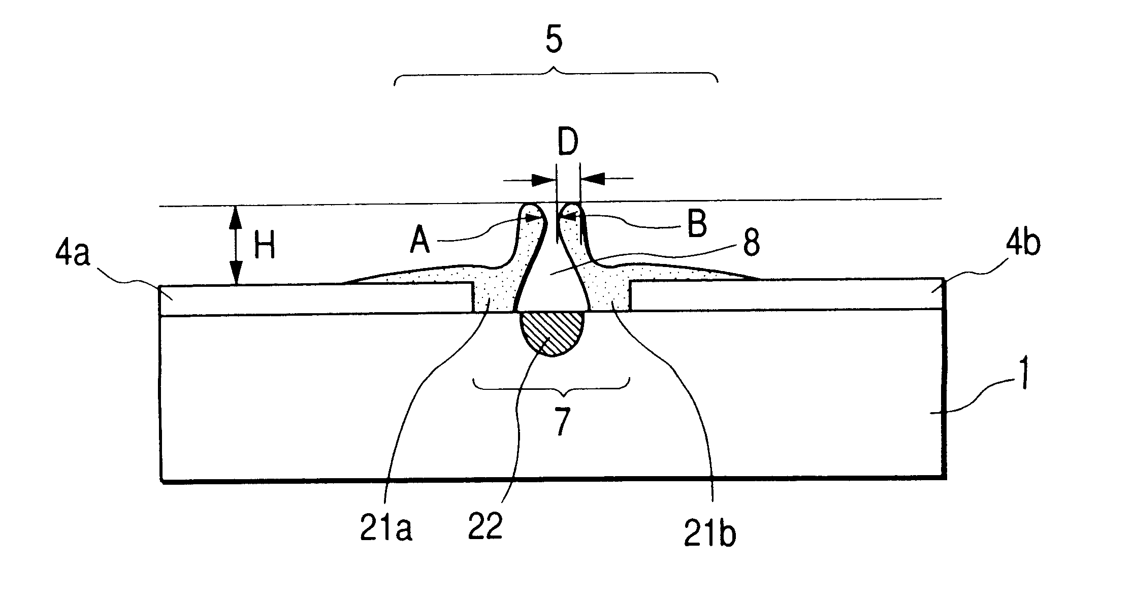
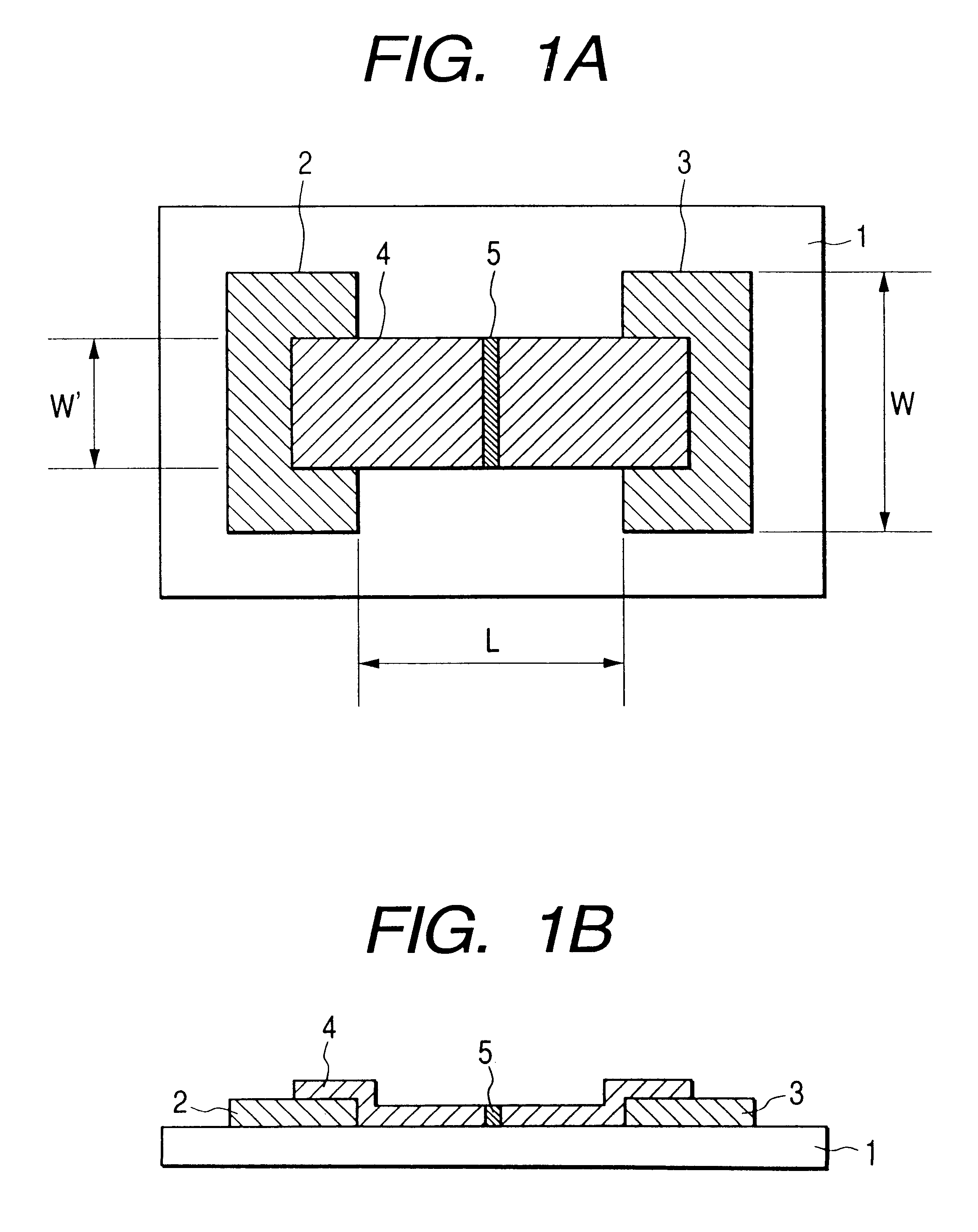
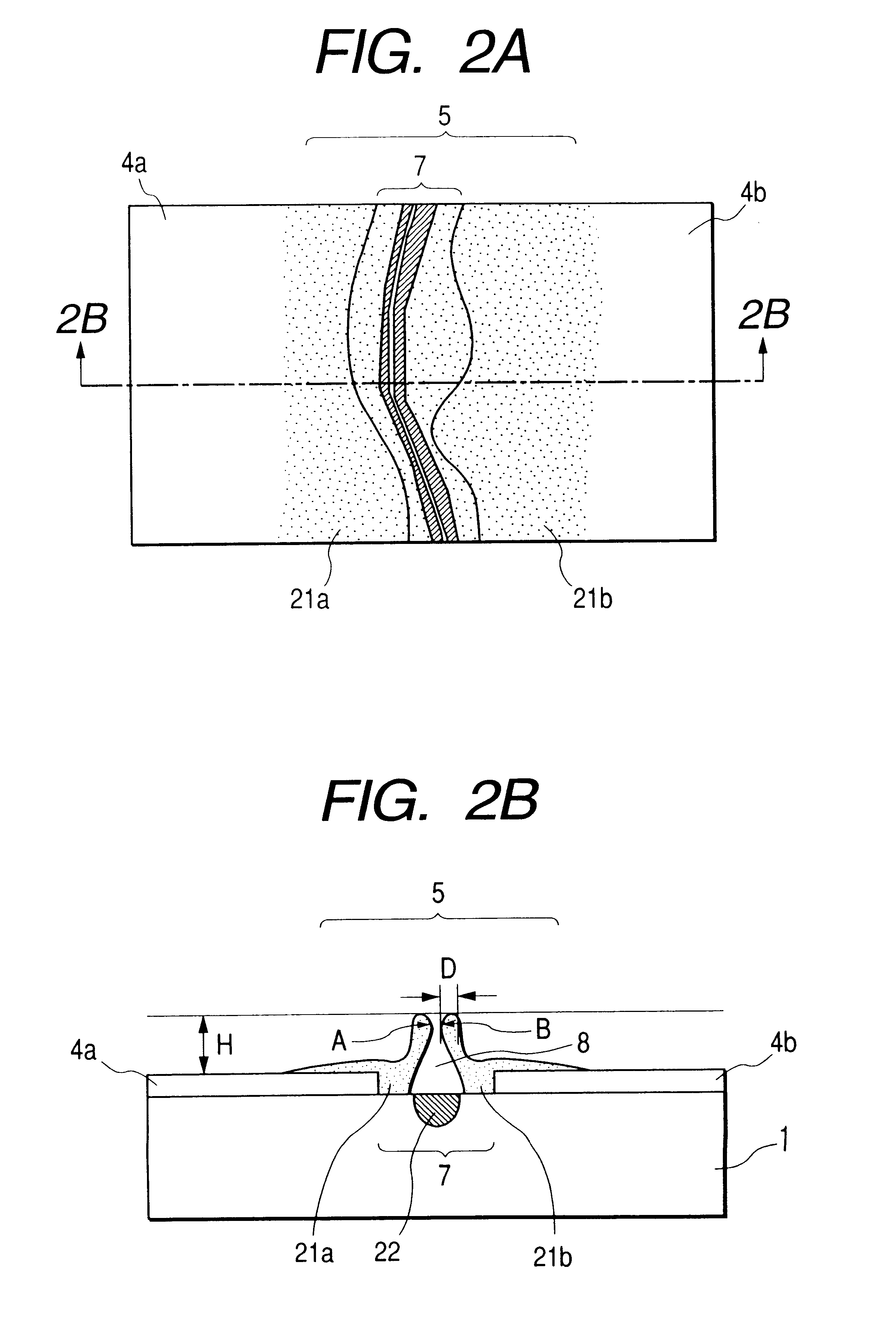
The basic structure of the electron-emitting device according to the present example is similar to that in the plan view and sectional view of FIGS. 1A and 1B and the enlarged plan view and sectional view of FIGS. 3A and 3B.
In the present example, the steps similar to those in Example 1 were carried out up to step-d.
(Step-e)
For carrying out the activation step next, tolunitrile was introduced through a slow leak valve into the vacuum chamber and the pressure of 1.3.times.10.sup.-4 Pa was maintained. Then the activation operation was carried out on the device after the forming operation by applying the voltage of the waveform illustrated in FIG. 8B through the device electrodes 2, 3 to the device under the conditions that T1 was 2 msec, T1' was 1 msec, T2 was 10 msec, and the maximum voltage was .+-.15 V. At this time the voltage supplied to the device electrode 3 was positive, and the device current If was positive along the direction of flow from the device electrode 3 to the devic...
example 4
The basic structure of the electron-emitting device according to the present example is similar to that in Example 3 and thus similar to that in the plan view and sectional view of FIGS. 1A and 1B and the enlarged plan view and sectional view of FIGS. 3A and 3B.
In the present example, the steps similar to those in Example 1 were carried out up to step-d.
(Step-e)
For carrying out the activation step next, acrylonitrile was introduced through the slow leak valve into the vacuum chamber and the pressure of 1.3.times.10.sup.-2 Pa was maintained. Then the activation operation was carried out on the device after the forming operation by applying the voltage of the waveform illustrated in FIG. 8B through the device electrodes 2, 3 to the device under the conditions that T1 was 1 msec, T1' was 0.5 msec, T2 was 10 msec, and the maximum voltage was .+-.14 V. At this time the voltage supplied to the device electrode 3 was positive, and the device current If was positive along the direction of f...
PUM
 Abstract
Description
Claims
Application Information