Composite laminate circuit structure and methods of interconnecting the same

a laminate circuit and laminate technology, applied in the field of laminate circuit structures, to achieve the effect of reducing costs and less costly

Inactive Publication Date: 2002-05-14
IBM CORP
View PDF12 Cites 85 Cited by
  • Summary
  • Abstract
  • Description
  • Claims
  • Application Information

AI Technical Summary

Benefits of technology

The present invention makes possible laminate circuit structures being more robust and less costly. The present invention provides for reduced cost since copper plating of the composite structure is no longer required...

Problems solved by technology

This requires precision drilling to form the plated through holes all of which is time consumi...

Method used


Image

  • Composite laminate circuit structure and methods of interconnecting the same
  • Composite laminate circuit structure and methods of interconnecting the same
  • Composite laminate circuit structure and methods of interconnecting the same

Examples


Embodiment Construction

In order to facilitate an understanding of the present invention, reference is made to the figures wherein the same numerals in different figures refer to the same or corresponding structures.

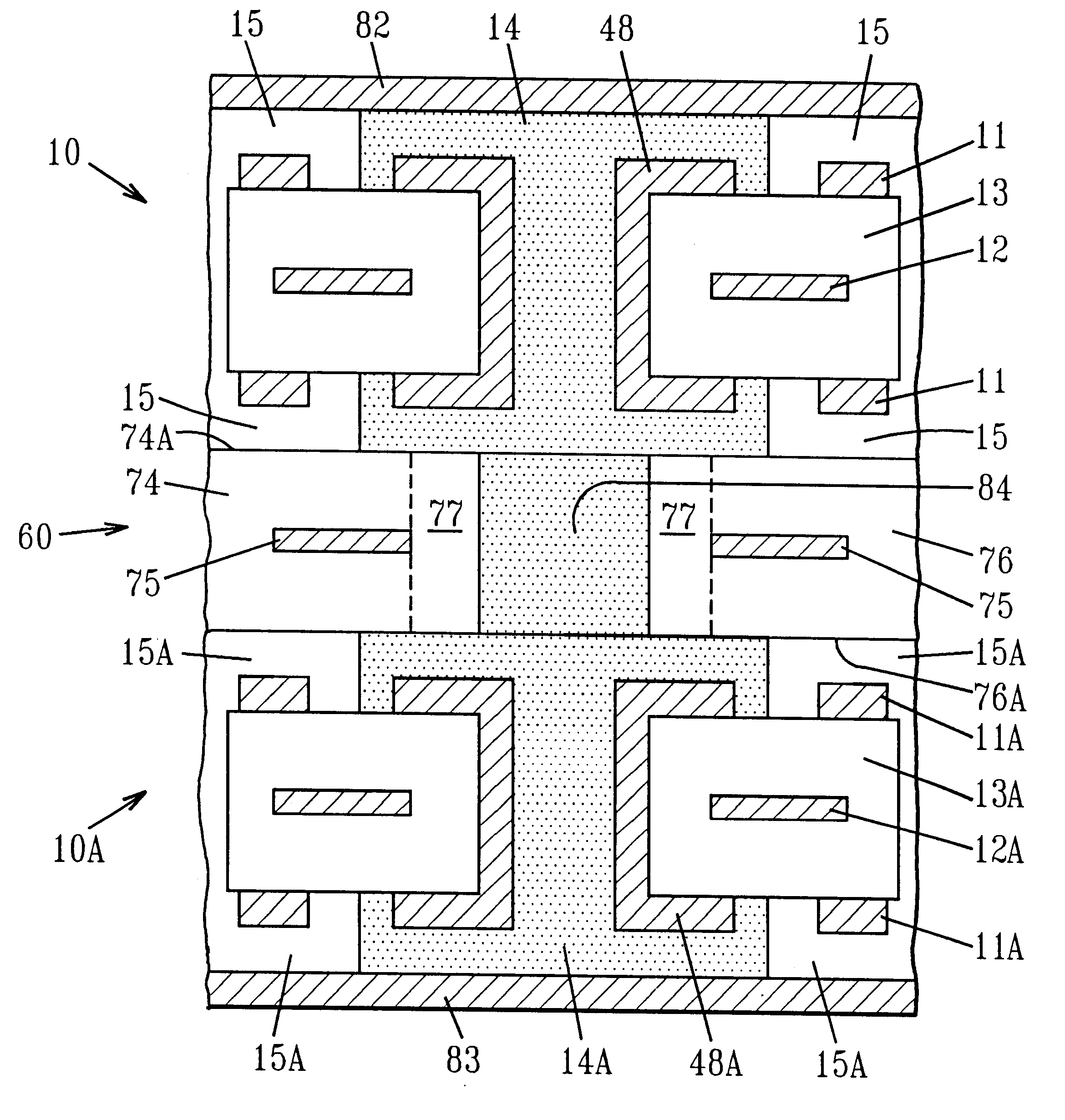
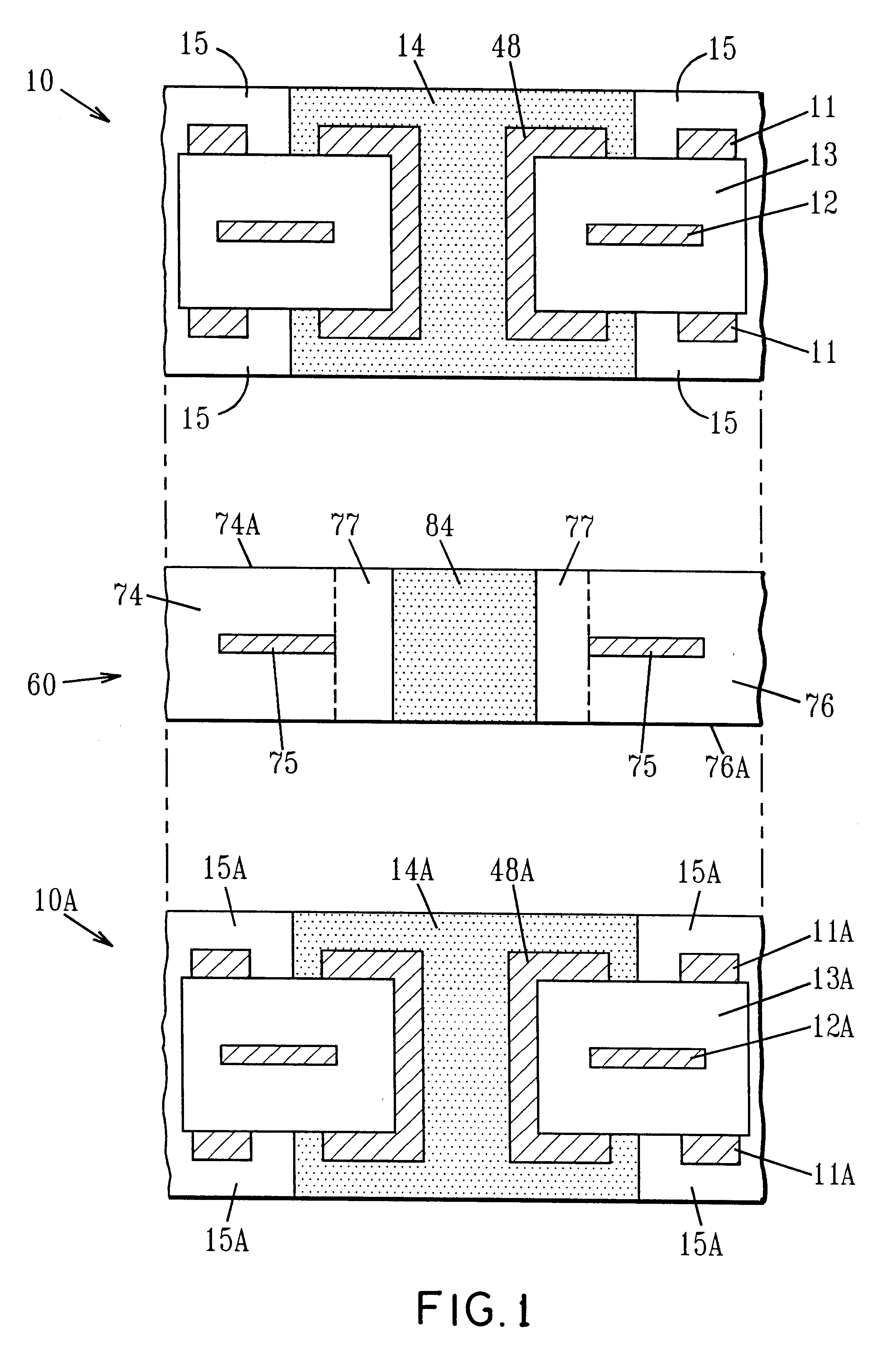
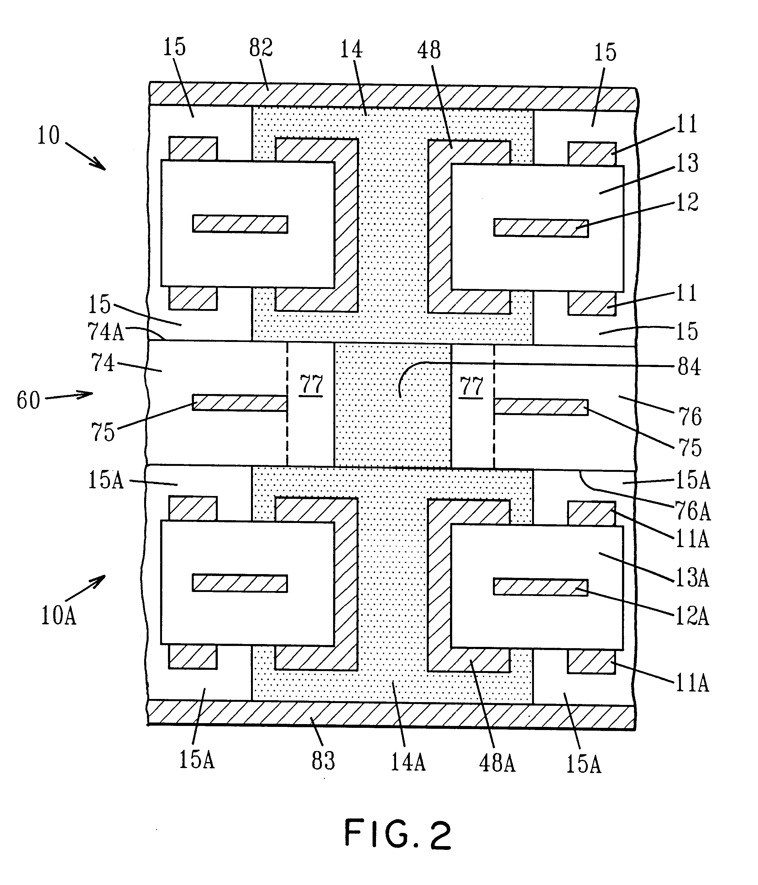
Reference to FIG. 1 illustrates two modularized circuitized plane subassemblies such as voltage planes 10, 10A. The subassemblies 10, 10A comprise at least two planes having circuit traces 11, 11A, for example signal planes, respectively disposed about an internal circuitized plane 12, 12A, respectively. The planes 12, 12A preferably can be voltage planes. The planes 11, 11A and 12, 12A are typically copper.

Dielectric material 13, 13A is located between the planes having circuit traces 11, 11A and planes 12, 12A. The dielectric material 13, 13A is typically any of the conventional dielectric materials used in fabricating signal and voltage planes such as epoxy glass compositions, FR-4 resins, polyfluorocarbons such as polytetrafluoroethylene, polyimides, polyamides, cyanate resins, and photoima...


PUM


Abstract

A laminate circuit structure assembly is provided that comprises at least two modularized circuitized plane subassemblies; a joining layer located between each of the subassemblies and wherein the subassemblies and joining layer are bonded together with a cured dielectric from a bondable, curable dielectric. The subassemblies and joining layer are electrically interconnected with bondable electrically conductive material. The joining layer comprises dielectric layers disposed about an internal electrically conductive layer. The electrically conductive layer has a via and the dielectric layers each have a via of smaller diameter than the vias in the electrically conductive layer and are aligned with the vias in the electrically conductive layer. The vias are filled with electrically bondable electrically conductive material for providing electrical contact between the subassemblies.

Description

DESCRIPTIONTechnical FieldThe present invention relates to laminate circuit structures, and more particularly to composite laminate circuit structures from a plurality of modularized circuitized plane subassemblies having a joining layer between each adjacent pair of subassemblies and being bonded together. The present invention also relates to a method for fabricating the laminate circuit structures. The present invention provides for planar, fine line external circuit flatlines and does not require plated through holes or copper plating of the composite structure.BACKGROUND OF INVENTIONA conventional technique of forming a laminate circuit board structures includes forming layers of dielectric material and electrically conducting material to provide multiple layers of circuits and voltage planes. Voltage planes can be either ground plane or power planes, and are sometimes collectively referred to as power planes. In one technique of forming such structure, layers of dielectric mat...

Claims


Application Information

Patent Timeline
IPC IPC(8): H01R4/26H01R4/00H05K3/46H05K3/00H05K3/40
CPCH01R4/26H05K3/462Y10T428/24917H05K3/4069H05K3/4623H05K3/4641H05K2201/0347H05K2201/09536H05K2201/0959H05K2201/096H05K2201/10378H05K2203/0307Y10S428/901Y10T156/1089H05K3/0023
Inventor LAUFFER, JOHN M.MARKOVICH, VOYA R.MILLER, THOMAS R.PAPATHOMAS, KONSTANTINOS I.WILSON, WILLIAM E.
Owner IBM CORP
Why Eureka
Try Eureka