Memory clock generation with configurable phase advance and delay capability

a technology of phase advance and delay capability, applied in the direction of generating/distributing signals, pulse techniques, instruments, etc., can solve the problems of affecting the overall timing budget of the memory interface, and the method is not flexible enough to allow the user

Inactive Publication Date: 2002-07-23
LINKEDIN
View PDF2 Cites 77 Cited by
  • Summary
  • Abstract
  • Description
  • Claims
  • Application Information

AI Technical Summary

Benefits of technology

The present invention provides a memory clock generation logic circuit comprising a configuration register including desired phase shift and time delay values, and circuitry for applying those values to a synchronization signal. The synchronization signal is shifted 0-, 90-, 180-, or 270-degrees according to the desired phase shift value. Additionally, the synchronization signal is delayed according to the desired time delay value. The combination of the phase shifting and the time delaying provides a method and an apparatus that allow for the fine tuning of the synchronization signal.

Problems solved by technology

Memory clock generation is a critical component of a memory subsystem implementation and affects the overall memory interface timing budget.
However, this method is not flexible enough to allow the user to compensate for board deficiencies and make a broader range of adjustments, given the strict timing requirements of emerging memory technologies such as DDR SDRAM and QDR SRAM.

Method used


Image

  • Memory clock generation with configurable phase advance and delay capability
  • Memory clock generation with configurable phase advance and delay capability
  • Memory clock generation with configurable phase advance and delay capability

Examples


Embodiment Construction

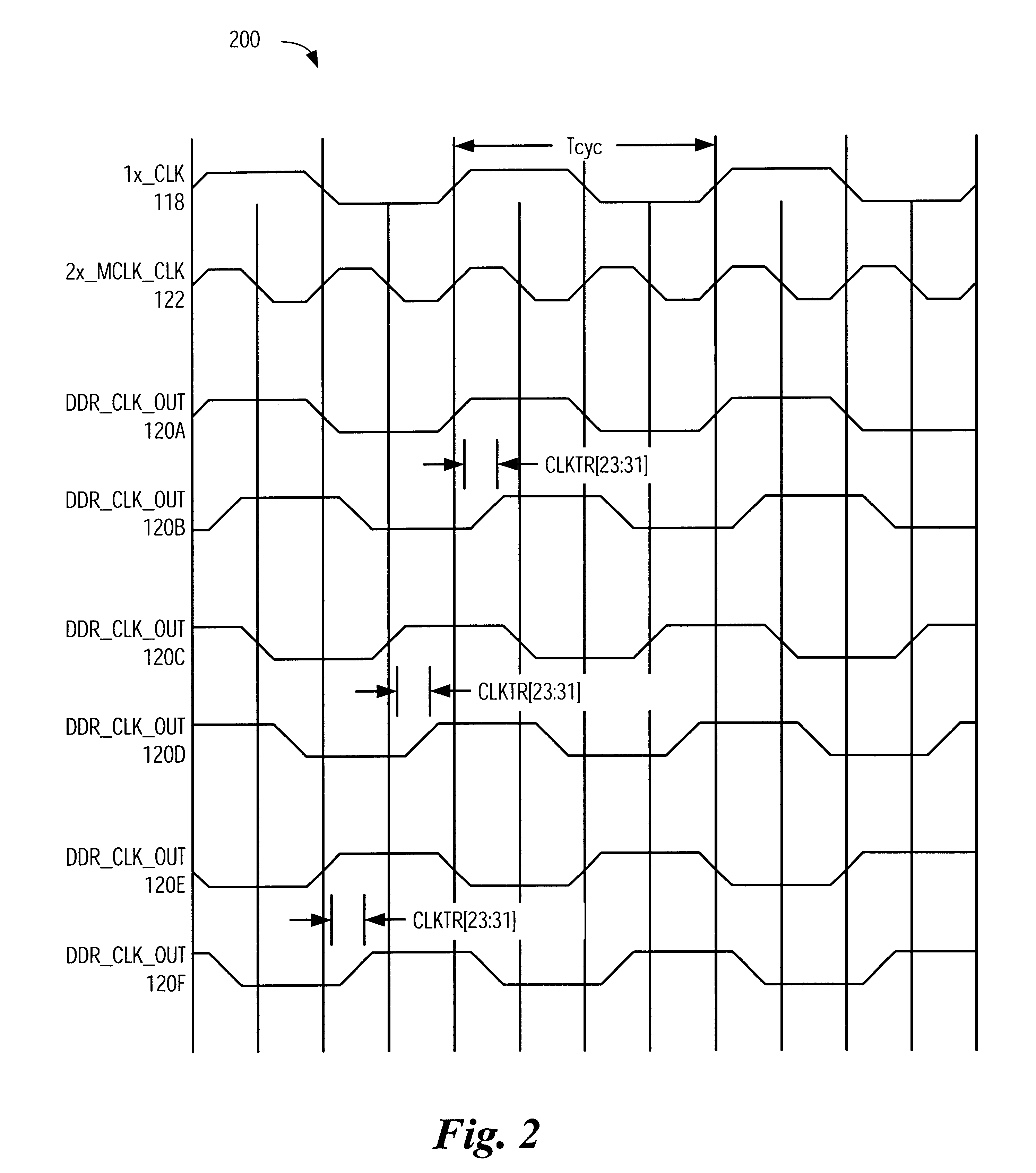
The principles of the present invention and their advantages are best understood by referring to the illustrated operations of the embodiments depicted in FIGS. 1-2.

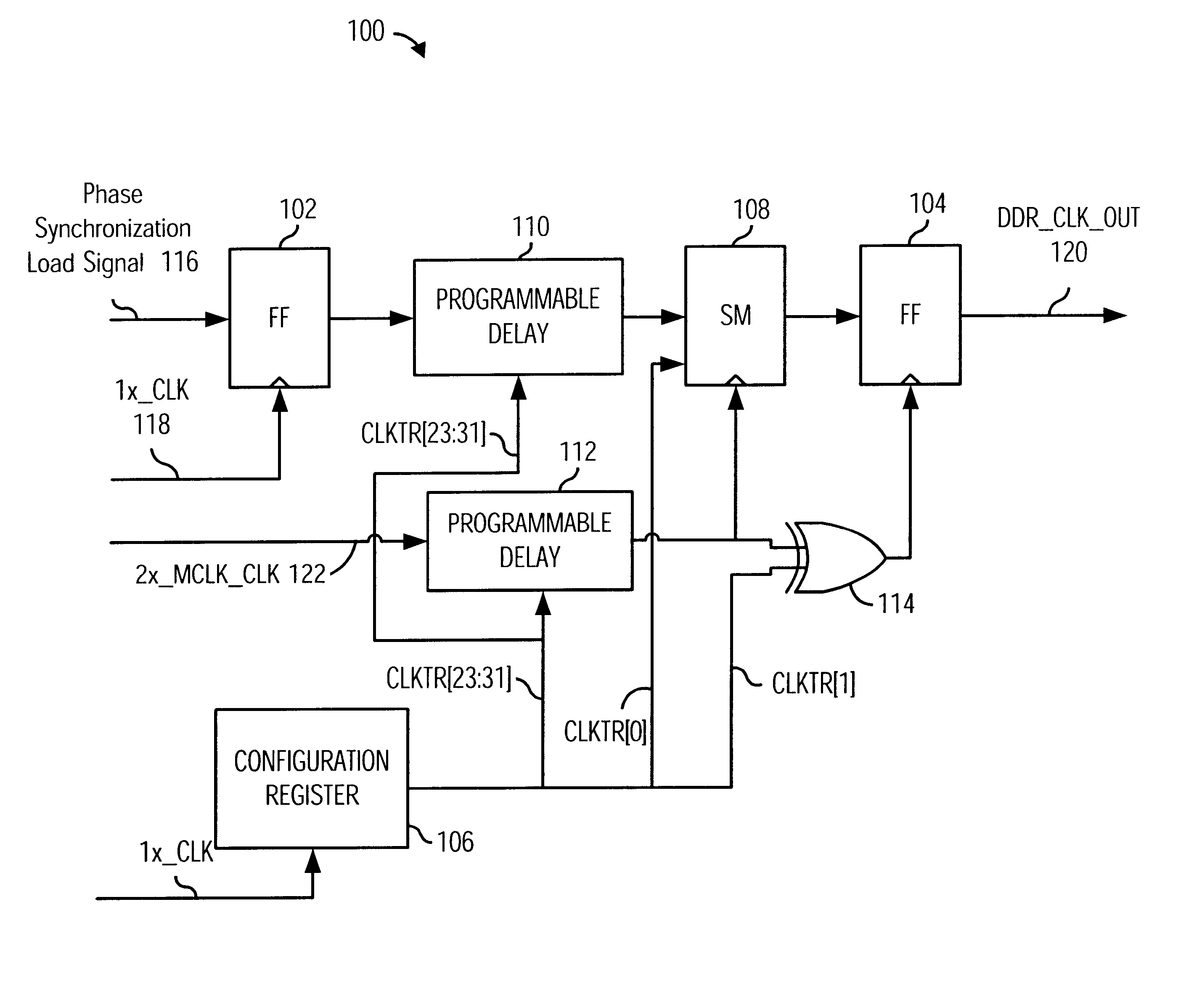
A preferred embodiment of the present invention is described in the memory clock generation logic circuit 100 as shown in FIG. 1. Preferably, the circuit 100 is implemented in a memory controller (not shown). The circuit 100 comprises two flip-flops (FFs) 102 and 104, a configuration register 106, a state machine (SM) 108, two programmable delays 110 and 112, and an XOR gate 114.

The FF 102 is configured for receiving the Phase Synchronization Load Signal 116 and the 1x_CLK 118 and for generating a timing signal that oscillates in the 1x_CLK domain. The 1x_CLK 118 is a clock signal of the same frequency as the memory controller internal clock frequency. The output of the FF 102 is connected to the input of the programmable delay 110, which is configured for accepting the timing signal from the FF 102 and a timing delay, r...


PUM


Abstract

A circuit generating memory clock with phase advance and delay capability is provided. The phase of the memory clock is controlled by adjusting the configuration register bits. The circuit allows for a high degree of control and flexibility in the memory clock generation in that the memory clock relationship with respect to the memory command and data can be adjusted independently, thereby creating the ability to effectively adjust the memory interface timings such as setup time, hold time, and memory read data access time. Specifically, 0, 90, and 180 degree phase advance ability is combined with the ability to add delay in fine increments to achieve a more granular degree of phase adjustment.

Description

BACKGROUND OF THE INVENTION1. Field of the InventionThe invention relates generally to memory clock generation and, more particularly, to memory clock generation with configurable phase advance and delay capability.2. Description of the Related ArtMemory clock generation is a critical component of a memory subsystem implementation and affects the overall memory interface timing budget. The memory subsystem clock generation and timing is particularly critical for existing memory technologies such as synchronous dynamic random access memory (SDRAM) and static random access memory (SRAM), and more so for emerging memory technologies, such as double data rate (DDR) SDRAM and quad data rate (QDR) SRAM, that employ source synchronous clocking schemes.Conventionally, memory clock adjustment support has been designed into the system board using fixed wire delay schemes to add or remove delay on the order of hundreds of pico seconds. However, this method is not flexible enough to allow the u...

Claims


Application Information

Patent Timeline
Patent Type & Authority Patents(United States)
IPC IPC(8): G06F1/10G11C7/22G11C7/00
CPCG06F1/10G11C7/1066G11C7/22G11C7/222
Inventor WOLFORD, BARRY JOE
Owner LINKEDIN
Why Eureka
Try Eureka