Semiconductor device with test circuit

a test circuit and semiconductor chip technology, applied in the direction of solid-state devices, semiconductor/solid-state device details, instruments, etc., can solve the problems of signal skew, affecting the test accuracy, and the inability to operate at intervals of a cycle time set for the installed semiconductor chips

Inactive Publication Date: 2002-08-06
KK TOSHIBA
View PDF4 Cites 16 Cited by
  • Summary
  • Abstract
  • Description
  • Claims
  • Application Information

AI Technical Summary

Problems solved by technology

As a result, the surface of the chip 102 is covered with the needles 51, to greatly reduce a space for accepting manual needles for the test, thereby hindering in the test of the defects analyzing.
The long bonding wires cause signal skew, and narrow gaps among the pads 40 hardly receive the bonding wires.
The boundary scan test circuit is configured to test the board at low test frequencies, and therefore, is unable to operate at intervals of a cycle time set for the semiconductor chips installed on the board.

Method used


Image

  • Semiconductor device with test circuit
  • Semiconductor device with test circuit
  • Semiconductor device with test circuit

Examples


first embodiment

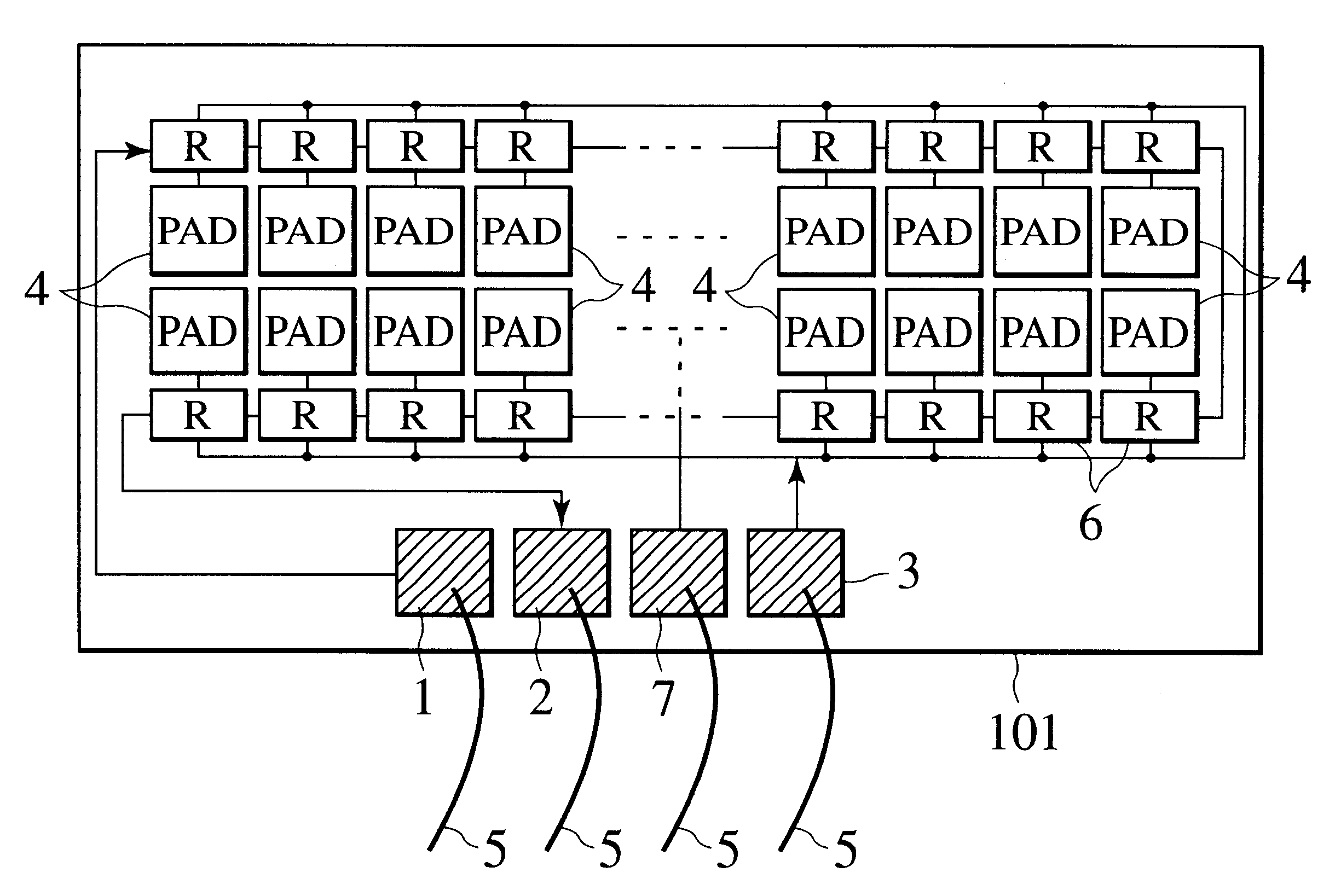
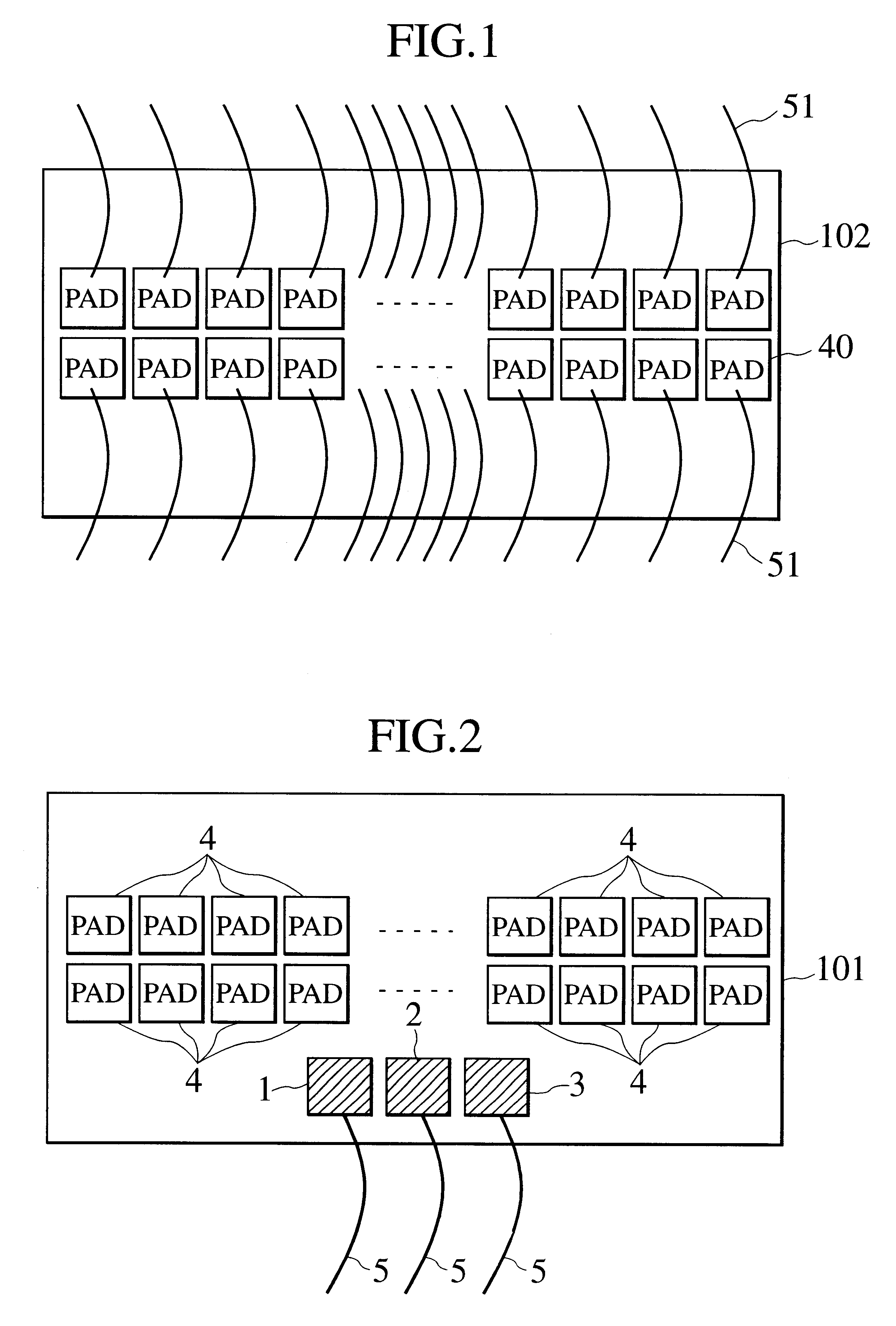
FIG. 2 is a block diagram showing a semiconductor device having I / O pads according to the first embodiment of the present invention. The semiconductor device is formed on a semiconductor chip 101. At the periphery of the chip 101, a test data input pad 1, a test data output pad 2, and a test clock signal (TCK) input pad 3 are formed. The pads 1 to 3 are connected to wires 5 used for a test such as a defects analyzing test. The wires 5 may be probe-card needles, bonding wires, etc. The I / O pads 4 are in a middle part of the chip 101.

An external tester (not shown) provides test data, which is serially set in the pads 4 through the test data input pad 1. After carrying out a predetermined test, the pads 4 provide resultant data, which is passed through a serial scan chain serving as a data path and is transferred to the external tester through the test data output pad 2. A test clock signal (TCK) used to transfer the test data is supplied from the external tester to the test clock sign...

second embodiment

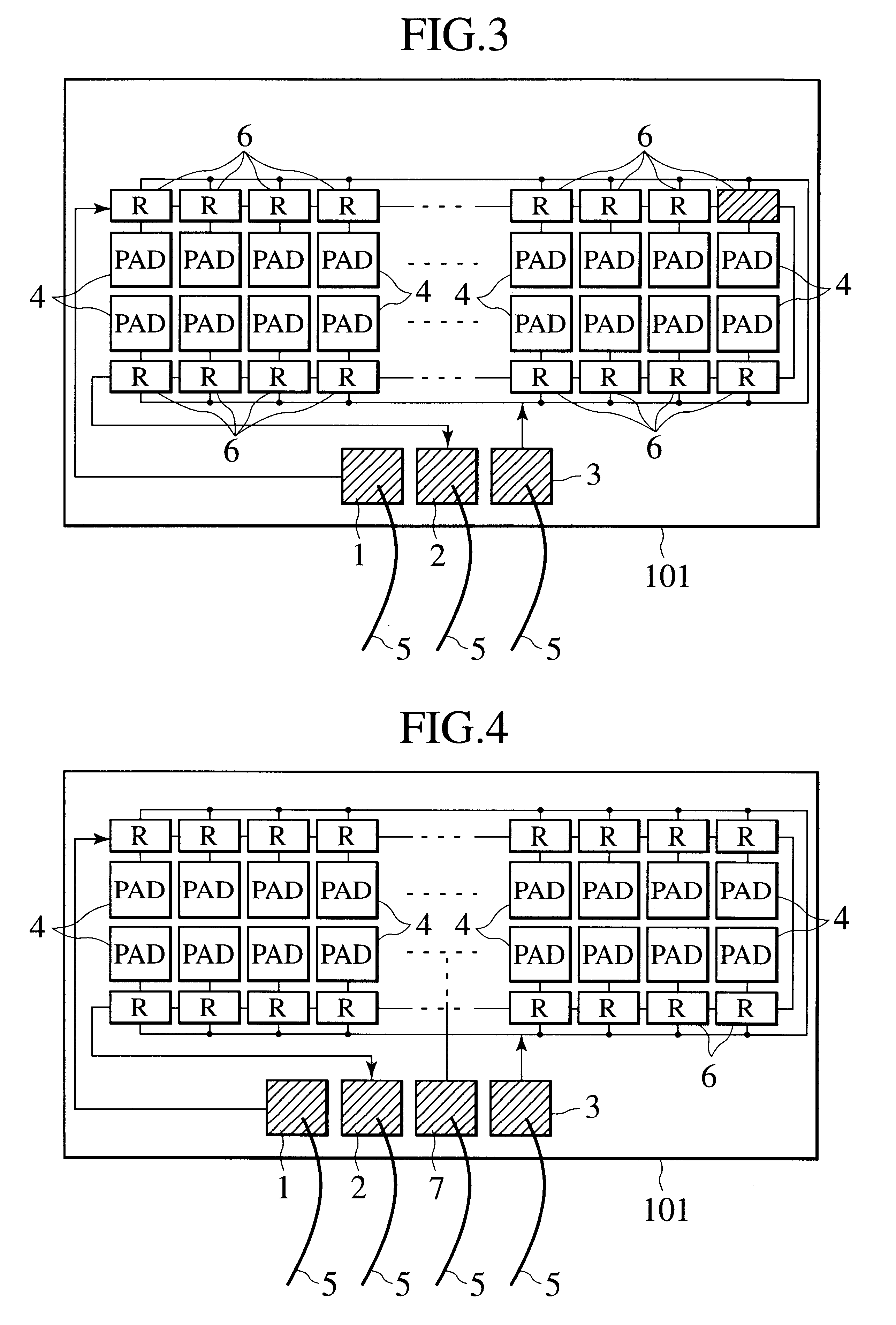
FIG. 8 is a block diagram showing a semiconductor device according to the second embodiment of the present invention. In FIG. 8, registers 6 and pads 4 and 41 correspond to the registers 6 forming a boundary scan chain and the pads 4 of FIG. 4. The pad 41 is a pad for which a test vector must be set according to a clock signal (CK) of a normal operation cycle time. A test vector generator 9 operating with the clock signal (CK) is arranged between the register 6 and the pad 41. The pads 4 are usual test pads having the registers 6, respectively. For the sake of simplicity of explanation, FIG. 8 shows only the pads 4 and 41 for receiving test data. For example, pads for providing test result data sent from internal circuits (not shown) to the outside are not shown in FIG. 8.

To set test data TDI in the pads 4 and 41 to carry out, for example, a defects analyzing test, an external tester (not shown) serially transfers the test data to the registers 6 of the pads in synchronization with ...

third embodiment

FIG. 9 is a block diagram showing a semiconductor device according to the third embodiment of the present invention. Each pad 41 is provided with a register group 81 containing "m" registers to supply a plurality of test vectors to the pad 41. The example of FIG. 9 has "n" pads 41 (n being a positive integer). If there are "m" test vectors, a matrix of "n.times.m" registers form a register circuit. In this case, the register circuit contains n register groups 81 each containing m registers. The register groups 81 correspond to the pads 41, respectively.

To set initial test data (TDI) in all registers of the register circuit, a multiplexer (MUX) 82 selects a test clock signal (TCK) according to a control signal TEST and supplies the selected test clock signal as a control signal A to the registers of each register group 81.

According to the control signal TEST, each multiplexer 83 receives the test data (TDI) from an external tester (not shown) and sequentially transfers the test data ...


PUM


Abstract

A semiconductor device has pads that are arranged in such a manner as to easily accept manual needles to carry out a test. This technique is applicable to carry out a test with use of a boundary scan test circuit in synchronization with a cycle time defined by a normal operation clock signal. The semiconductor device has a first pad connected to a first one of registers that form a serial scan chain, to supply test data to the registers, a second pad connected to a last one of the registers, and a third pad to supply a test clock signal to the registers. The registers are arranged in a central part of the semiconductor device, and the first to third pads are arranged at the periphery of the semiconductor device.

Description

This application claims benefit of priority under 35 USC 119 based on Japanese Patent Application No. P2000-175484 filed on Jun. 12, 2000, the entire contents of which are incorporated by reference herein.1. Field of the InventionThe present invention relates to a semiconductor device with a test circuit and pads that are arranged to easily carry out a test such as a defects analyzing test, and a semiconductor device capable of carrying out a test at intervals of a cycle time set for a semiconductor chip.2. Description of Related ArtFIG. 1 is a block diagram showing pads arranged on a semiconductor chip in a semiconductor device. The pads and are arranged in a middle part of the chip 102 in order to improve circuit performance. In FIG. 1, the pads are input / output (I / O) pads 40 and are connected to probe-card needles or bonding wires 51, respectively.To carry out a test such as a defects analyzing test on the semiconductor device, a probe card, for example, is used. The probe card h...

Claims


Application Information

Patent Timeline
Patent Type & Authority Patents(United States)
IPC IPC(8): G01R31/28G01R31/3185H01L21/822H01L27/04
CPCG01R31/318538H01L24/06H01L2224/05554H01L2224/48091H01L2924/00014H01L2924/14H01L2924/00
Inventor HATADA, HIROSHIOTSUKA, NOBUAKIHIRABAYASHI, OSAMUKAMEDA, YASUSHI
Owner KK TOSHIBA
Why Eureka
Try Eureka