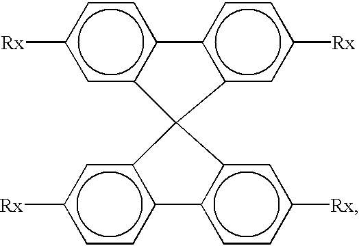
Organic luminescence device with spiro compound
a luminescence device and organic technology, applied in the direction of organic semiconductor devices, discharge tubes/lamp details, natural mineral layered products, etc., can solve the problems of deterioration, affecting the performance of luminescence devices, and insufficient durability of luminescence devices
- Summary
- Abstract
- Description
- Claims
- Application Information
AI Technical Summary
Benefits of technology
Problems solved by technology
Method used
Image
Examples
examples 2-20
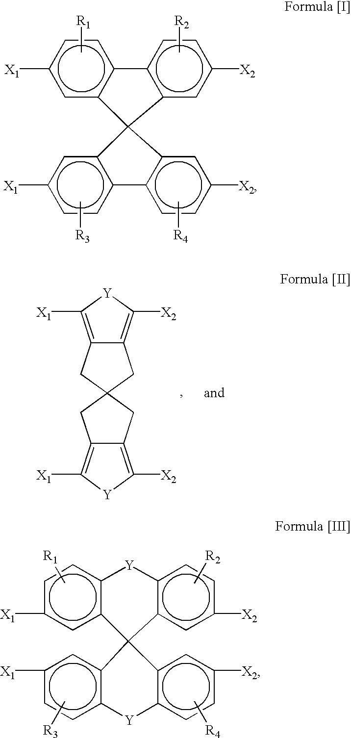
Organic luminescence devices were prepared and evaluated in the same manner as in Example 1 except for replacing the spiro compound of Compound No. I-4 with Compounds Nos. I-6, I-7, I-10, I-13, I-21, I-25, II-1, II-5, II-7, II-10, II-12, II-15, II-23, II-28, II-33, III-4, III-7, III-9 and III-11, respectively, listed in Tables 1 to 3 set forth above.
The results are inclusively shown in Table 4 set forth hereinafter.
example 21
The procedure of Example 1 was repeated up to the formation of the hole-transporting layer 5.
Then, the hole-transporting layer 5 was further coated by vacuum deposition of a mixture of spiro compound (Compound No. I-1) and aluminum tris(quinolinol) in a weight ratio of 1:20 to form a 60 nm-thick electron-transporting layer 6 under a vacuum of 1.0.times.10.sup.-4 Pa and at a film thickness growth rate of 0.2-0.3 nm / sec.
Then, the electron-transporting layer was further coated by vacuum deposition of Al--Li alloy (Li content: 1 atom. %) to form a 150 nm-thick metal film 4 under a vacuum of 1.0.times.10.sup.-4 Pa and at a film thickness growth rate of 1.0-1.2 nm / sec, thereby forming an organic luminescence device of a structure shown in FIG. 2.
The thus-obtained device was then supplied with a DC voltage of 8 volts between the ITO electrode 2 as an anode and the Al--Li alloy electrode as a cathods, whereby a current flowed at a density of 8.7 mA / cm.sup.2 and red luminescence was observed...
examples 22-32
Organic luminescence devices were prepared and evaluated in the same manner as in Example 21 except for replacing the spiro compound of Compound No. I-1 with Compounds Nos. I-8, I-11, I-16, I-23, II-2, II-9, II-16, II-20, III-2, III-6 and III-7, respectively, listed in Tables 1 to 3 set forth above.
The results are inclusively shown in Table 5 set forth hereinafter.
PUM
| Property | Measurement | Unit |
|---|---|---|
| thickness | aaaaa | aaaaa |
| thickness | aaaaa | aaaaa |
| thickness | aaaaa | aaaaa |
Abstract
Description
Claims
Application Information


