Method of manufacturing an electro-optical device

Inactive Publication Date: 2002-10-15
SEMICON ENERGY LAB CO LTD
View PDF16 Cites 159 Cited by
  • Summary
  • Abstract
  • Description
  • Claims
  • Application Information

AI Technical Summary

Benefits of technology

In the above two electro-optical devices, the use of the gap retaining members provides the following advantages. First, it is no longer necessary to use spacers. Second, since the height of the gap retaining members can be set as desired, the interval between the substrates can be determined as desired. Third, since the gap retaining members are fixed, they are not gathered unlike the conventional spacers. Therefore, point defects do not occur.
In the above two electro-optical devices, the position of the gap retaining members can be set as desired. For example, the gap retaining members can be provided in an area that substantially confronts the pixel area. In this case, it is preferable that the gap retaining members be provided at locations that are not used for display, for instance, on a black matrix of color filters and bus lines in the pixel area. Alternatively, by providing the gap retaining members in an area that does not confront the pixel area, the interval between the substrates can be retained without causing any influences on the display.
Where the invention

Problems solved by technology

However, the liquid crystal display device having the above configuration has the following problems.
As a result, the driver circuit TFTs having a more complex structure than the pixel TFTs are damaged considerably, which adversely affects the yield of products.
As described above, where the cell gap is controlled by using conventional grainy spacers, satisfactory display may not be obtained due to various factors.
In liquid crystal

Method used


Image

  • Method of manufacturing an electro-optical device
  • Method of manufacturing an electro-optical device
  • Method of manufacturing an electro-optical device

Examples


Example

Embodiment 1

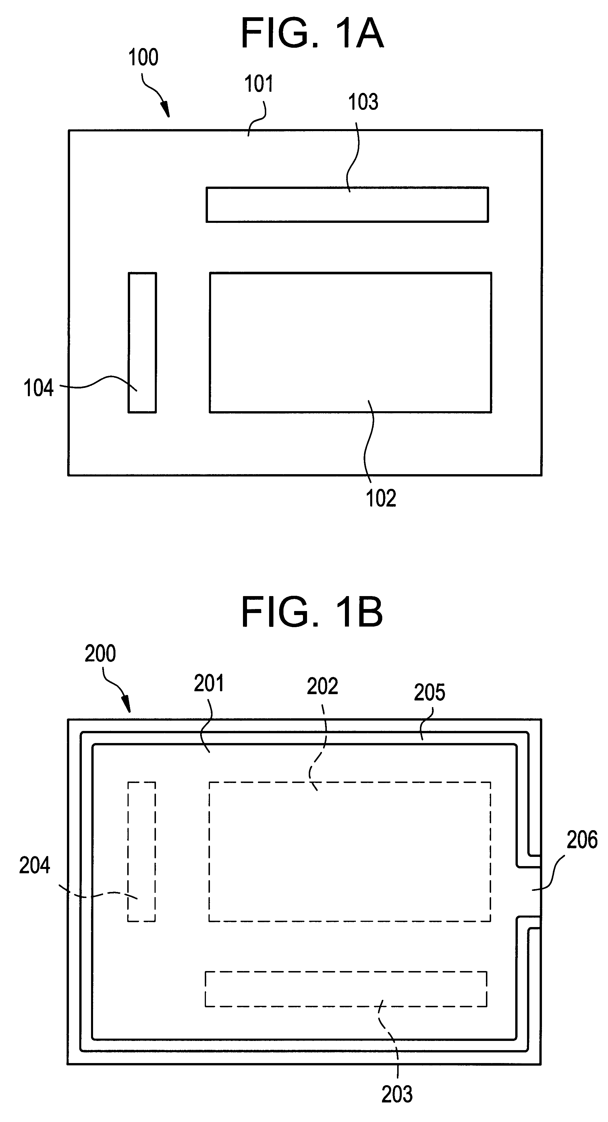
This embodiment will be described with reference to FIGS. 1A-1B to 6. This embodiment is directed to a case where the invention is applied to an active matrix liquid crystal display device. FIG. 1A is a top view of a TFT substrate and FIG. 1B is a top view of an opposed substrate.

As shown in FIG. 1A, a TFT substrate 100 consists of a substrate 101 and a pixel area 102 and driver circuit areas 103 and 104 that are formed on the substrate 101. Pixel electrodes, TFTs that are connected to the respective pixel electrodes, and other members are arranged in the pixel area 102. Driver circuits for driving the TFTs in the pixel area 102 are arranged in the driver circuit areas 103 and 104.

As shown in FIG. 1B, an opposed substrate 200 consists of a substrate 201, an area 202 to confront the pixel area 102 of the TFT substrate 100, and areas 203 and 204 to confront the respective driver circuit areas 103 and 104. The TFT substrate 100 and the opposed substrate 200 are bonded toget...

Example

Embodiment 2

In this embodiment, the steps until pixel TFTs and driver circuit TFTs are formed to constitute a TFT substrate are the same as in the first embodiment and hence are not described here.

After the pixel TFTs and the driver circuit TFTs are formed in an integral manner to constitute the TFT substrate, gap retaining members are formed on the TFT substrate as shown in FIG. 3B. A process of forming gap retaining members according to this embodiment will be described below with reference to FIGS. 7A-7D and 8A-8C. The configuration of FIG. 7A is the same as that of FIG. 4A.

First, as shown in FIG. 7B, a 2.2-.mu.m-thick photosensitive polyimide film 311 is formed by spin coating. Thereafter, the substrate is left at the room temperature for 30 minutes to uniformize the thickness of the photosensitive polyimide film 311 over the entire TFT substrate 100 (leveling). Then, the TFT substrate 100 on which the photosensitive polyimide film 311 is formed is pre-baked at 120.degree. C. fo...

Example

This embodiment is different from the first embodiment only in the number and arrangement of gap retaining members. Since this embodiment is the same as the first or second embodiment in the other points, a manufacturing process will not be described. In FIG. 10, the same reference numerals as in FIGS. 1A and 1B and FIG. 9 denote the same members as in the latter figures. In this embodiment, a sealing agent 403 is formed on the TFT substrate 100 side.

In this embodiment, as shown in FIG. 10, gap retaining members 401 are formed on the TFT substrate 100 so as to surround the pixel area 102 and gap retaining members 402 are formed on the TFT substrate 100 so as to surround the driver circuit areas 103 and 104. The gap retaining members 401 and 402 are shaped like a cylinder of 30 .mu.m in diameter and 2.2 .mu.m in height.

Then, rubbing is performed on the surface of the opposed substrate 200, i.e., the surface of an alignment film, and a sealing agent 403 is applied to the TFT substrate...


PUM


Abstract

In an active matrix semiconductor display device in which pixel TFTs and driver circuit TFT are formed on the same substrate in an integral manner, the cell gap is controlled by gap retaining members that are disposed between a pixel area and driver circuit areas. This makes it possible to provide a uniform cell thickness profile over the entire semiconductor display device. Further, since conventional grainy spacers are not used, stress is not imposed on the driver circuit TFTs when a TFT substrate and an opposed substrate are bonded together. This prevents the driver circuit TFTs from being damaged.

Description

BACKGROUND OF THE INVENTION1. Field of the InventionThe present invention relates to a semiconductor display device using thin-film transistors. In particular, the invention relates to a semiconductor display device in which a pixel switching circuit and driver circuits are formed on the same substrate in an integral manner.2. Description of the Related ArtIn recent years, the techniques of forming semiconductor devices, such as thin-film transistors (TFTs), by using a semiconductor thin film formed on an inexpensive glass substrate have made rapid progress. This is because of increased demand for active matrix liquid crystal display devices.In active matrix liquid crystal display devices, TFTs are provided for respective ones of hundreds of thousands to millions of pixel regions that are arranged in matrix and charge that enters or exits from each pixel electrode is controlled by the switching function of the associated TFT.The basic configuration of an active matrix liquid crystal...

Claims


Application Information

Patent Timeline
IPC IPC(8): G02F1/13G02F1/1362H01L21/70H01L27/12H01L21/84G02F1/1339H01L21/77
CPCG02F1/13454H01L27/12H01L27/1214H01L27/1248G02F1/1339
Inventor HIRAKATA, YOSHIHARUNISHI, TAKESHIYAMAZAKI, SHUNPEI
Owner SEMICON ENERGY LAB CO LTD
Why Eureka
Try Eureka