Distributed feedback semiconductor laser device

a semiconductor laser and feedback technology, applied in the direction of lasers, semiconductor lasers, optical resonator shapes and construction, etc., can solve the problems of peltier devices, temperature dependence, and low stability of dfb lasers of the second conventional exampl

Inactive Publication Date: 2002-10-29
FURUKAWA ELECTRIC CO LTD
View PDF3 Cites 12 Cited by
  • Summary
  • Abstract
  • Description
  • Claims
  • Application Information

AI Technical Summary

Benefits of technology

In accordance with the first invention, the DFB semiconductor laser device having a higher side mode suppression ratio can be provided which stably operates in a wider range of injection current when external reflection light is incident by proving the diffraction grating formed by the GaInNAs(Sb) having the composition for efficiently absorbing light which has the laser emission wavelength of the active layer.

Problems solved by technology

The spectrum stability of the DFB laser of the second conventional example was not high.
The GaInAsP-based semiconductor laser includes a problem that a temperature characteristic of a threshold value or a characteristic temperature "To" which is a factor showing the temperature dependency of the threshold value is as low as 50 to 70 K. In other words, the temperature dependency is worse and a cooling device such as a Peltier device is required.
As described in the second conventional example, the range of realizing the single mode is narrow and the DFB laser is unstable to external reflection rays.
However, due to the lattice-mismatching, the GaInAs layer having the In content of about 30% and thickness of about 50 mm can be hardly grown with the higher quality crystal growth.

Method used


Image

  • Distributed feedback semiconductor laser device
  • Distributed feedback semiconductor laser device
  • Distributed feedback semiconductor laser device

Examples


Embodiment Construction

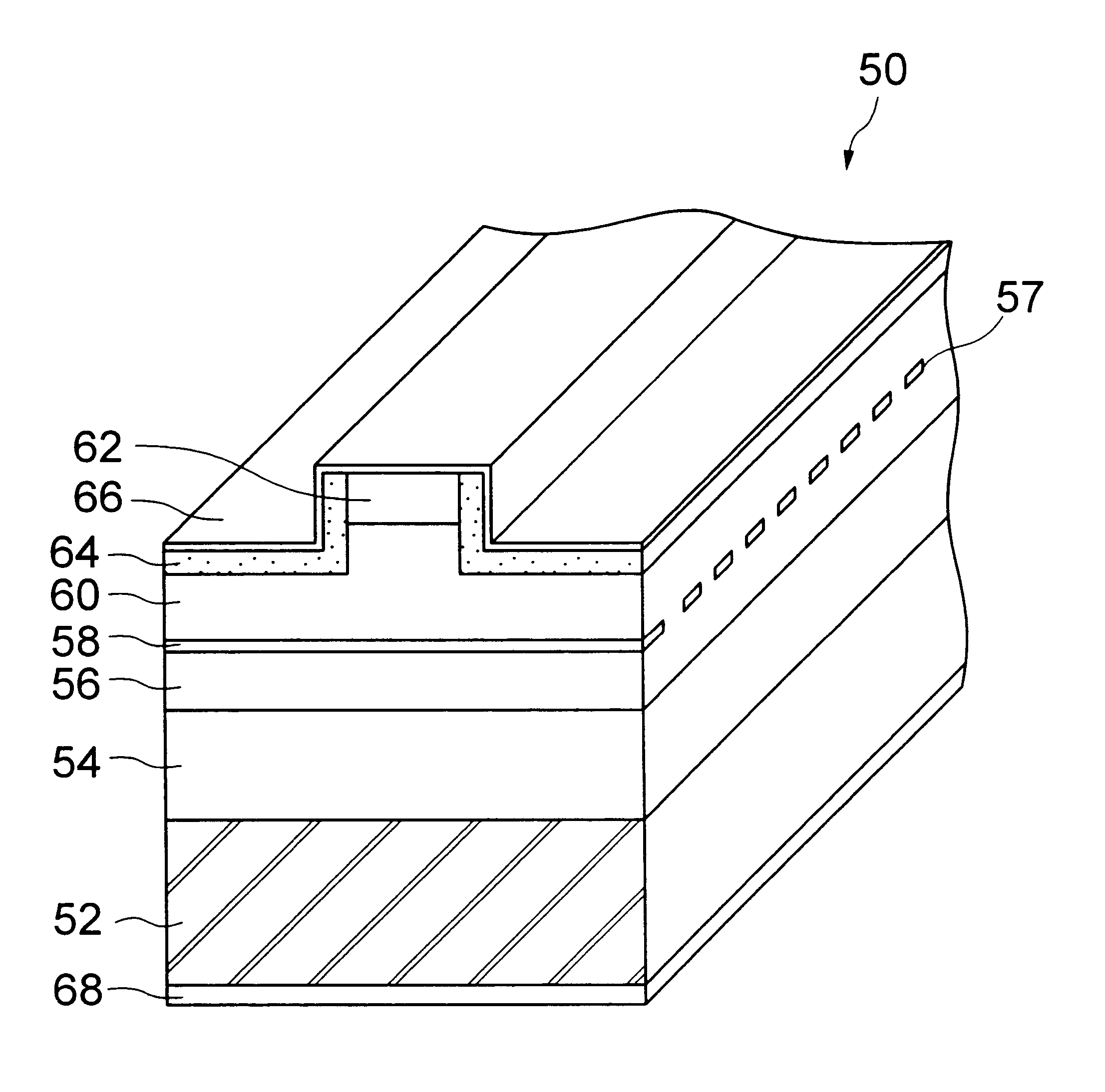
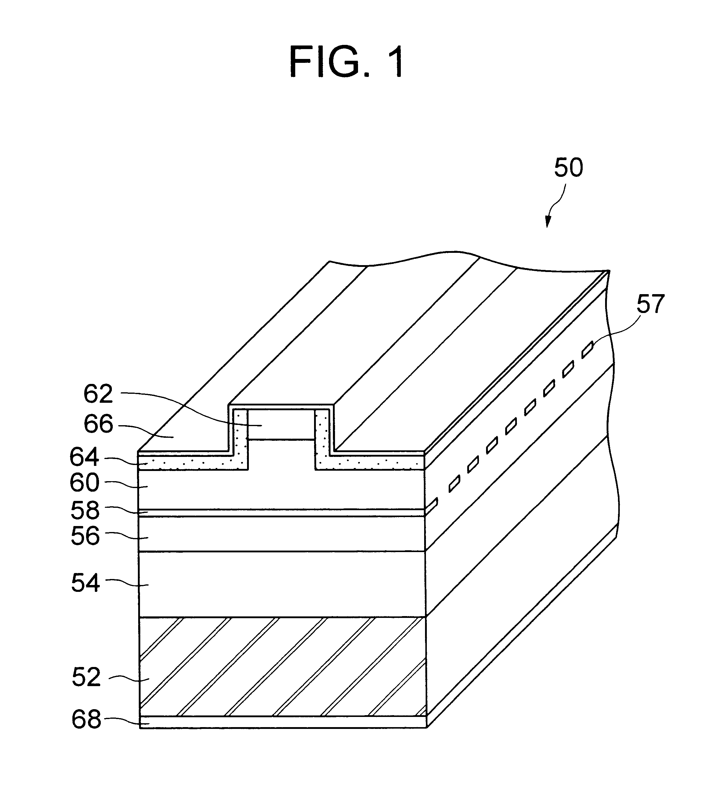
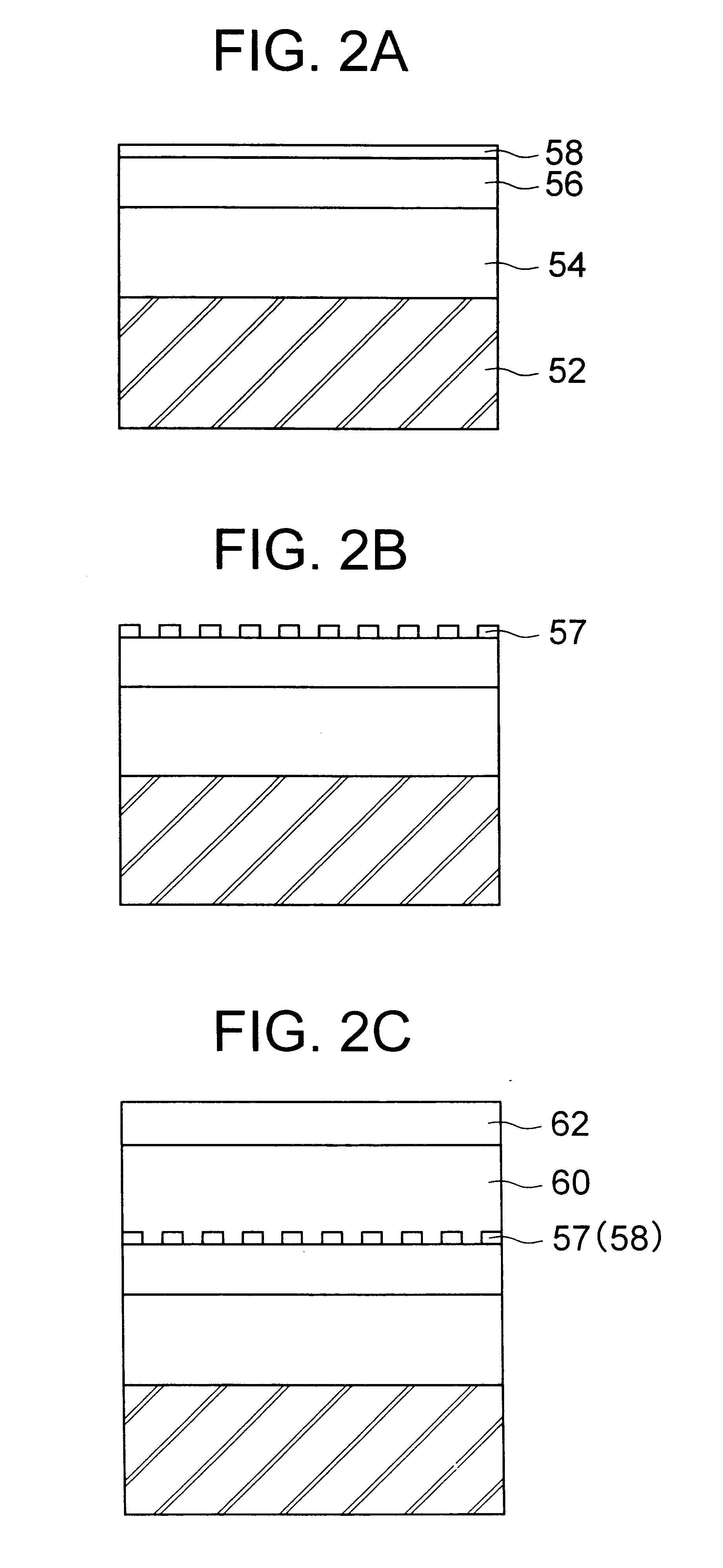
Then, the configuration of a semiconductor laser device of an embodiment in accordance with the first invention will be described referring to FIG. 1 and FIGS. 2A to 2C.

As shown in FIG. 1, a semiconductor laser device 50 is a ridge waveguide and absorption-type distributed feedback semiconductor laser device (DFB laser) and includes a stacked structure obtained by sequentially depositing an n-AlGaAs cladding layer 54 having a thickness of 2 .mu.m, an InGaAs / GaAs quantum well structure layer 56, a GaInNAs absorption layer 58 having a diffraction grating 57, a p-AlGaAs cladding layer 60 having a thickness of 2 .mu.m and a GaAs capping layer 62 having a thickness of 0.3 .mu.m overlying an n-GaAs substrate 52 having a thickness of 100 .mu.m.

The GaInNAs absorption layer 58 containing 6% of In and 2% of N has a composition that is lattice-matched with GaAs substrate, and the diffraction grating 57 having a cycle of 140 nm are disposed in the GaInNAs absorption layer 58.

In the stacked stru...


PUM


Abstract

A DFB semiconductor laser device including: a semiconductor substrate; and an active layer and a diffraction grating overlying the semiconductor substrate, the diffraction grating having a composition of GaInNAs(Sb) and absorbing light having a laser emission wavelength of the active layer. The DFB semiconductor laser device having a higher SMSR can be provided which stably operates in a wider range of injection current by proving the diffraction grating formed by the GaInNAs(Sb) having the composition for efficiently absorbing light which has the laser emission wavelength of the active layer.

Description

BACKGROUND OF THE INVENTION(a) Field of the InventionThe present invention relates to a distributed feedback (DFB) semiconductor laser device having a longer wavelength band between 0.9 and 1.65 .mu.m frequently used as a light source for optical communication, more in detail to the DFB semiconductor laser device having a stable emission wavelength and being operatable at a single wavelength especially suitable for exciting an optical fiber amplifier or a Raman amplifier, and to the Peltier-fee DFB semiconductor laser device having smaller temperature dependency.(b) Description of the Related ArtA DFB semiconductor laser device has a stable laser emission wavelength and is operated at a single wavelength especially suitable for use in wave-lenght-multiplexing (WDM) systems and high-bit-rate transmission and so on.As the first conventional example, the configuration of a 980 nm-band InGaAs-based semiconductor laser device used as an excitation light source for an optical fiber amplif...

Claims


Application Information

Patent Timeline
Patent Type & Authority Patents(United States)
IPC IPC(8): H01S5/323H01S5/00H01S5/12
CPCH01S5/1228H01S5/3235H01S5/12H01S5/1231H01S5/32366H01S5/32391
Inventor MUKAIHARA, TOSHIKAZUSHIMIZU, HITOSHIFUNABASHI, MASAKIKASUKAWA, AKIHIKO
Owner FURUKAWA ELECTRIC CO LTD
Why Eureka
Try Eureka