Process improvement for the creation of aluminum contact bumps

a technology of contact bumps and aluminum, which is applied in the direction of semiconductor devices, semiconductor/solid-state device details, electrical devices, etc., can solve the problems of increasing the negative impact of circuit performance, chip performance can be significantly degraded, and the capacitance of these wires is higher

Inactive Publication Date: 2002-11-12
TAIWAN SEMICON MFG CO LTD
View PDF3 Cites 29 Cited by
  • Summary
  • Abstract
  • Description
  • Claims
  • Application Information

AI Technical Summary

Problems solved by technology

The metal connections, which connect the Integrated Circuit to other circuit or system components, have therefore become of relative more importance and potentially have, with the further miniaturization of the IC, an increasingly negative impact on the cir

Method used


Image

  • Process improvement for the creation of aluminum contact bumps
  • Process improvement for the creation of aluminum contact bumps
  • Process improvement for the creation of aluminum contact bumps

Examples


Embodiment Construction

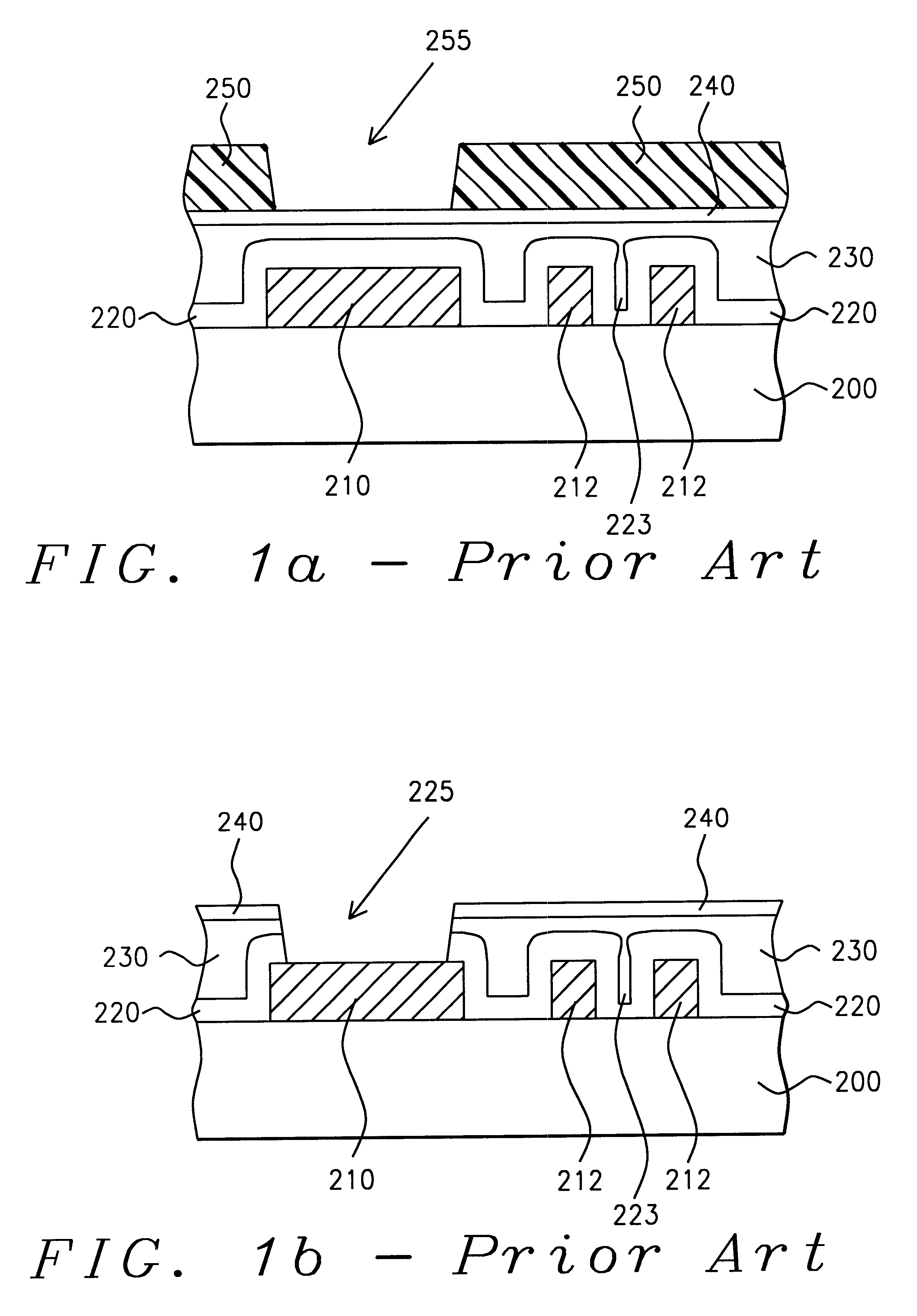
For reasons of ease of understanding and for comparison purposes, a prior method of creating aluminum solder bumps will first be highlighted. This method is following Chien et al. U.S. Pat. No. 6,130,149, FIGS. 1a through 1f are used for this purpose.

FIG. 1a shows a cross section of a substrate 200 on which are provided: 210, a patterned layer of metal that can comprise aluminum or copper; patterned metal layer 210 provides a point of electrical contact on the surface of substrate 200 and is connected to at least one of the semiconductor devices (not shown) that have been created in or on the surface of substrate 200 212, a pattern of interconnect lines that is adjacent to the patterned metal layer 210; 220, a layer of passivation deposited over the surface of substrate 200; it must be noted that the surface of layer 220 follows the contours of the surfaces of the patterned layer 210 of metal and the interconnect lines 212; under the Chien et al. invention, the main objective is to ...


PUM


Abstract

A new method is provided for the creation of an aluminum bump on a surface of a semiconductor device. A patterned layer of aluminum overlying a substrate is created, the patterned layer of aluminum is the layer of aluminum over which a contact bump is to be created. A layer of passivation is deposited, a first layer of photoresist is deposited for the creation of an opening in the layer of passivation that partially exposed the surface of the patterned layer of aluminum. This patterned first layer of photoresist remains in place, a layer of aluminum is sputter deposited, a second layer of photoresist is deposited which is patterned and etched for the creation of the aluminum bump overlying the patterned layer of aluminum. The aluminum solder bump is created by etching the deposited layer of aluminum. After the solder bump has been created, the patterned first and the second layers of photoresist are removed in one processing step, leaving in place the solder bump.

Description

BACKGROUND OF THE INVENTION(1) Field of the InventionThe invention relates to the fabrication of integrated circuit devices, and more particularly, to a improved method of providing aluminum contact bumps on a semiconductor surface.(2) Description of the Prior ArtThe conventional method that is used for the creation of semiconductor devices simultaneously creates numerous devices and device features on the surface of a semiconductor substrate, after the devices in or on the surface of the substrate have been completed the substrate is cut (diced) for the formation of individual die. The device circuitry that is internal to the device is connected to device input / output (I / O) points of electrical contact. These I / O points of electrical contact to the die must, after the individual die has been created, be further connected to either other semiconductor devices or to a packaging interface. A completed and diced semiconductor die can be connected at a first or card level, which can be ...

Claims


Application Information

Patent Timeline
IPC IPC(8): H01L21/02H01L21/60H01L23/485H01L23/48
CPCH01L24/11H01L24/13H01L2224/13099H01L2924/01005H01L2924/01011H01L2924/01013H01L2924/01022H01L2924/01029H01L2924/01059H01L2924/01078H01L2924/01079H01L2924/04941H01L2924/14H01L2924/30105H01L2924/3025H01L2924/01006H01L2924/01019H01L2924/01024H01L2924/01033H01L2924/014H01L2224/13124H01L2924/00014H01L2924/0001H01L24/05H01L2224/05147H01L2224/05171H01L2224/05573H01L2224/0558H01L2224/45144H01L2924/00H01L2224/05647
Inventor HUANG, KUN-MINGLEE, CHENG-WEIYU, DING-JENG
Owner TAIWAN SEMICON MFG CO LTD
Why Eureka
Try Eureka