Continuous deposition process and apparatus for manufacturing cadmium telluride photovoltaic devices

a photovoltaic device and continuous deposition technology, applied in the direction of sustainable manufacturing/processing, final product manufacturing, vacuum evaporation coating, etc., can solve the problems of limiting the short circuit current (jsub>sc/sub>) of the solar cell, further complicated, and low optical transmission coefficient of approximately 80%, so as to increase the grain size of the absorber layer

Inactive Publication Date: 2010-07-22
CHEN YUNG TIN
View PDF8 Cites 57 Cited by
  • Summary
  • Abstract
  • Description
  • Claims
  • Application Information

AI Technical Summary

Benefits of technology

[0028]According to yet another aspect of the present invention, a method for fabricating a heterojunction photovoltaic device comprises the steps of providing an optically transparent substrate coated with a transparent conductive oxide layer thereon; depositing an n-type window layer onto the transparent conductive oxide layer by sputter deposition; depositing a p-type CdTe absorber layer doped with chlorine or iodine onto the window layer; and annealing the absorber layer by a plurality of rapid thermal anneal (RTA) lamps at a temperature in the range of from about 450° C. to about 600° C. to thereby increase the grain size of the absorber layer. The n-type window layer is formed of an n-type semiconductor selected from the group consisting of CdS, CdS:Cl, Cd1-xZnxS and Cd1-xZnxS:Cl, where x ranges from more than zero to no more than one. The p-type absorber layer is formed of CdTe:Cl or CdTe:I. The substrate is continuously conveyed in the successive processing steps without being exposed to the atmospheric environment.
[0029]To achieve the above and other objects, according to still another aspect of the present invention, a modular deposition apparatus for depositing semiconductor compounds containing tellurium or sulfur as a principal constituent on substrates to form photovoltaic devices as the substrates are

Problems solved by technology

However, SnO2:F has a relatively low optical transmission coefficient of approximately 80%, which limits the short circuit current (Jsc) of the solar cell.
This is further complicated by the fact that some CdS is consumed during the subsequent CdTe deposition and post-deposition annealing.
There has been a trend to minimize the thickness of the CdTe absorber layer 27 in order to conserve the rare element tellurium (Te), because it is thought that there may not be adequate Te supply to fabricate enough CdTe photovoltaic devices to meet global demand.
If the work function of the contact does not exceed that of the p-type CdTe, a Schottky barrie

Method used


Image

  • Continuous deposition process and apparatus for manufacturing cadmium telluride photovoltaic devices
  • Continuous deposition process and apparatus for manufacturing cadmium telluride photovoltaic devices
  • Continuous deposition process and apparatus for manufacturing cadmium telluride photovoltaic devices

Examples


Embodiment Construction

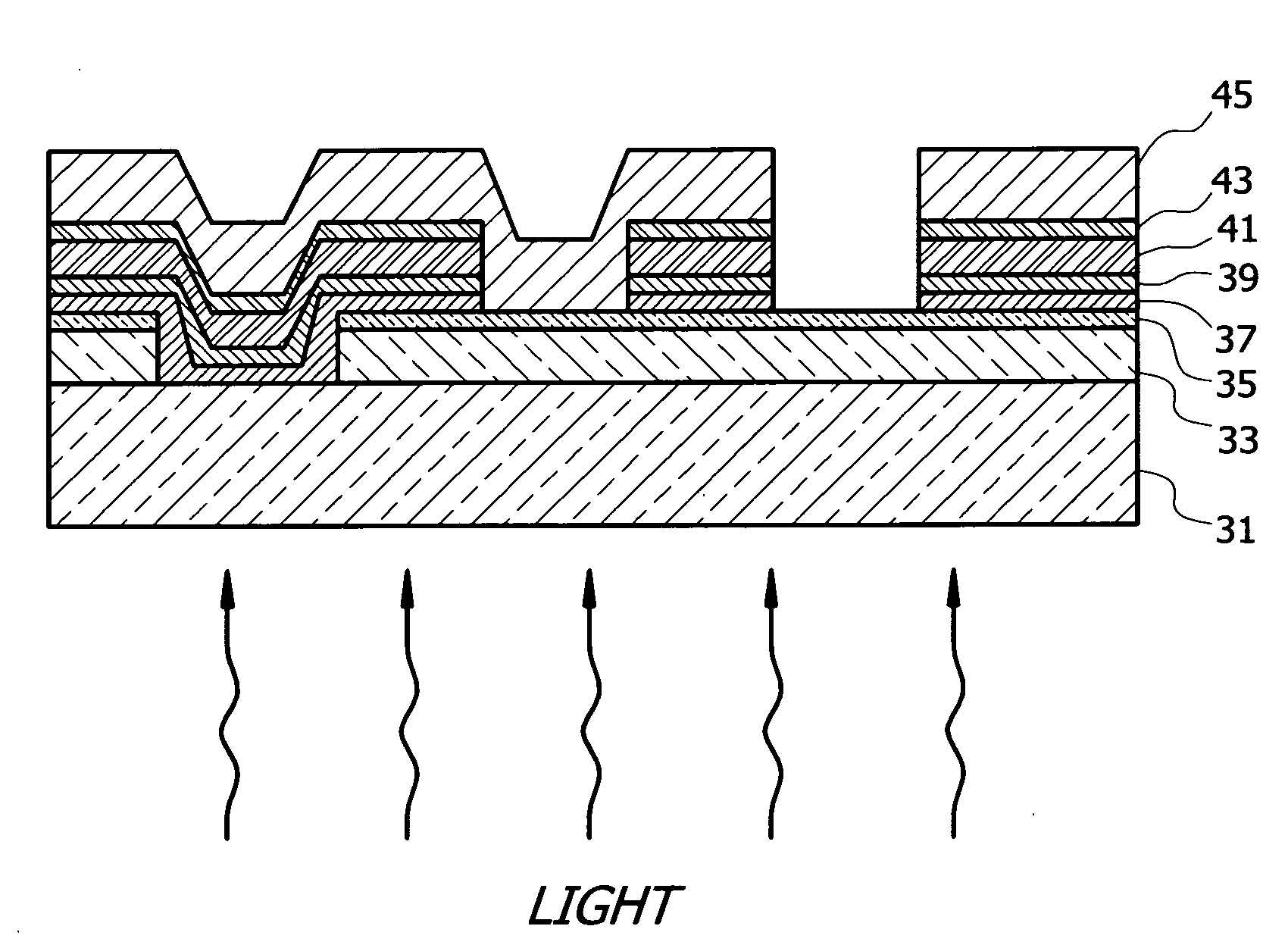
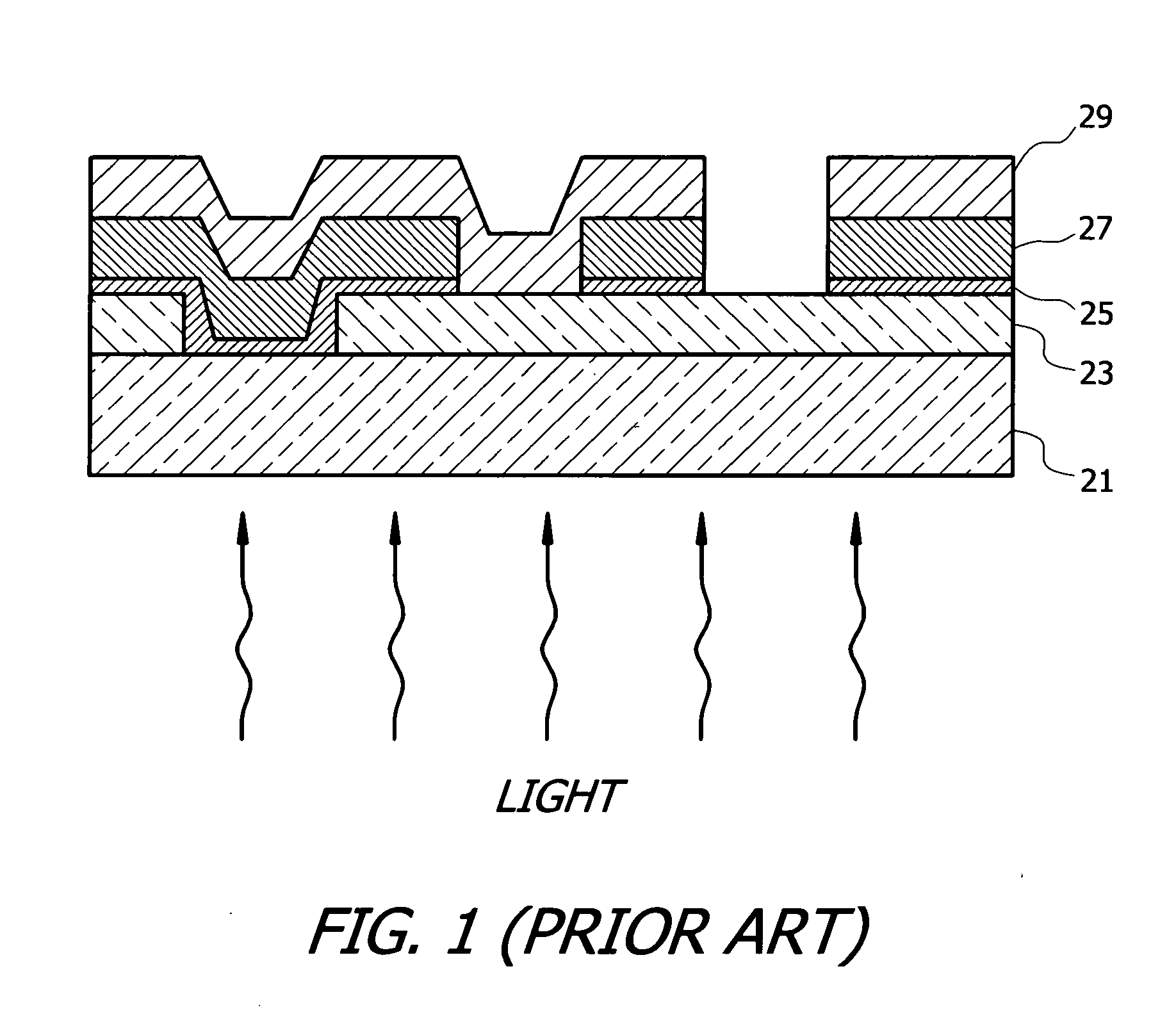
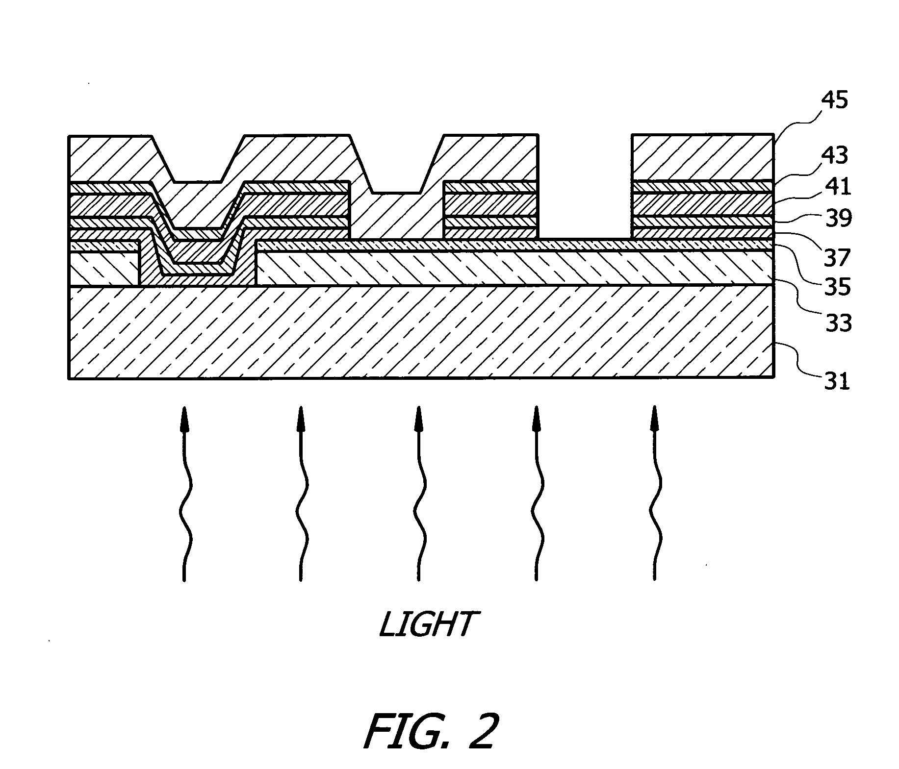
[0039]The present invention overcomes the inability of the conventional CdTe photovoltaic device to absorb low energy photons by the spectrum splitting or multi band gap approach, wherein multiple absorber layers with different band gap energies are employed to absorb photons from a wider range of the solar spectrum. Compared with the conventional CdTe absorber having a band gap energy of 1.45-1.5 eV, an absorber layer with a higher band gap energy can convert high energy photons to higher open circuit voltage (Voc), while an absorber with a lower band gap energy can absorb lower energy photons and allow more efficient use of the solar spectrum.

[0040]The preferred embodiment of the present invention as applied to a CdTe photovoltaic device having three absorber layers will now be described with reference to FIG. 2. Referring now to FIG. 2, the illustrated device has an optically transparent dielectric substrate 31, through which radiant energy or sunlight enters the device; a layer ...


PUM


Abstract

A continuous deposition process and apparatus for depositing semiconductor layers containing cadmium, tellurium or sulfur as a principal constituent on transparent substrates to form photovoltaic devices as the substrates are continuously conveyed through the deposition apparatus is described. The film deposition process for a photovoltaic device having an n-type window layer and three p-type absorber layers in contiguous contact is carried out by a modular continuous deposition apparatus which has a plurality of processing stations connected in series for depositing successive layers of semiconductor films onto continuously conveying substrates. The fabrication starts by providing an optically transparent substrate coated with a transparent conductive oxide layer, onto which an n-type window layer formed of CdS or CdZnS is sputter deposited. After the window layer is deposited, a first absorber layer is deposited thereon by sputter deposition. Thereafter, a second absorber layer formed of CdTe is deposited onto the first absorber layer by a novel vapor deposition process in which the CdTe film forming vapor is generated by sublimation of a CdTe source material. After the second absorber layer is deposited, a third absorber layer formed of CdHgTe is deposited thereon by sputter deposition. The substrates are continuously conveyed through the modular continuous deposition apparatus as successive layers of semiconductor films are deposited thereon.

Description

RELATED APPLICATIONS[0001]The present application is a continuation-in-part application of U.S. provisional patent application, Ser. No. 61 / 205,560, filed Jan. 21, 2009, for HYBRID SPUTTERING AND VAPOR TRANSPORT DEPOSITION PROCESS FOR MULTIPLE BAND-GAPPED CADMIUM TELLURIDE PHOTOVOLTAIC DEVICES, by Yung-Tin Chen, included herein by reference and for which benefit of the priority date is hereby claimed.FIELD OF THE INVENTION[0002]The present invention relates to a process and apparatus for manufacturing photovoltaic devices and more particularly to the process and apparatus for depositing thin film layers for cadmium telluride photovoltaic devices on a continuously conveying substrate.BACKGROUND OF THE INVENTION[0003]Photovoltaic technology offers great potential as an alternative source of electrical energy. Among various types of thin film solar cell technologies, cadmium telluride (CdTe) semiconductor based solar cells have emerged to be one of the leading candidates for large scal...

Claims


Application Information

Patent Timeline
IPC IPC(8): H01L31/0352C23C14/34C23C16/54H01L31/0216
CPCH01L31/02963H01L31/0725H01L31/073H01L31/1836Y02E10/543Y02P70/521Y02P70/50
Inventor CHEN, YUNG-TIN
Owner CHEN YUNG TIN
Why Eureka
Try Eureka