Resputtered copper seed layer

a seed layer and copper technology, applied in the direction of vacuum evaporation coating, coating, electric discharge tube, etc., can solve the problems of narrowest portion of sidewall portion thickness, and difficult to achieve sufficient via sidewall coverage. , to achieve the effect of low argon pressure, low coil power and high target power

Inactive Publication Date: 2008-08-14
APPLIED MATERIALS INC
View PDF5 Cites 59 Cited by
  • Summary
  • Abstract
  • Description
  • Claims
  • Application Information

AI Technical Summary

Benefits of technology

[0016]The sputter deposition and etch process may be repeated to fill more of the hole before copper electroplating. If the sputter and etch process are repeated sufficiently, the hole may be filled with copper by the last deposition step to fill the hole so that chemical mechanical polishing may immediately follow the sputter deposition.
[0017]The sputter deposition and etch processes may be performed in a single plasma sputter chamber. For example, the chamber may be equipped with an RF coil. Sputter deposition is favored at low argon pressure, high target power, and low coil power. Sputter etching is favored at higher argon pressure, lower target power, and higher coil power. The substrate should be strongly biased for at least the initial copper deposition steps and for the argon sputter etching steps.

Problems solved by technology

Filling metallization and especially liner layers into the high aspect-ratio holes presents great challenges.
If the copper seed layer 30 is relatively thick, the overhangs 38 grow and the throat 40 shrinks, thereby increasing the effective aspect ratio for sputtering into the via hole 18 with the result that it is difficult to achieve sufficient via sidewall coverage.
However, the thickness of the narrowest portion of the sidewall portion 34 may be insufficient and the sidewall portion 34 may become discontinuous to form gaps to expose the underlying barrier material, which poorly nucleates ECP copper.
While the extent of the overhangs may be somewhat reduced, if the overhangs are pushed below the level of the field barrier, the overhang etching may expose a facet of the barrier layer at the corner of the via hole and etch through it, thereby locally destroying the barrier.
Further but related problems arise when the dielectric material is a carbon-containing low-k dielectric material such as Black Diamond II available from Applied Materials, Inc. of Santa Clara, Calif.
Such materials do not afford the highly anisotropic etch available in silica.
The problems worsen when the dielectric material is made porous to further decrease the dielectric constant.
Yet further, the vertical structure to be etched through during the dielectric etch process may be more complicated than previously illustrated.

Method used


Image

  • Resputtered copper seed layer
  • Resputtered copper seed layer
  • Resputtered copper seed layer

Examples


Embodiment Construction

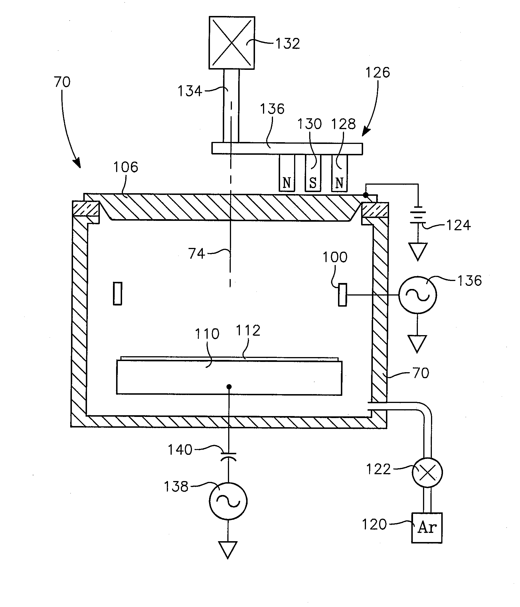
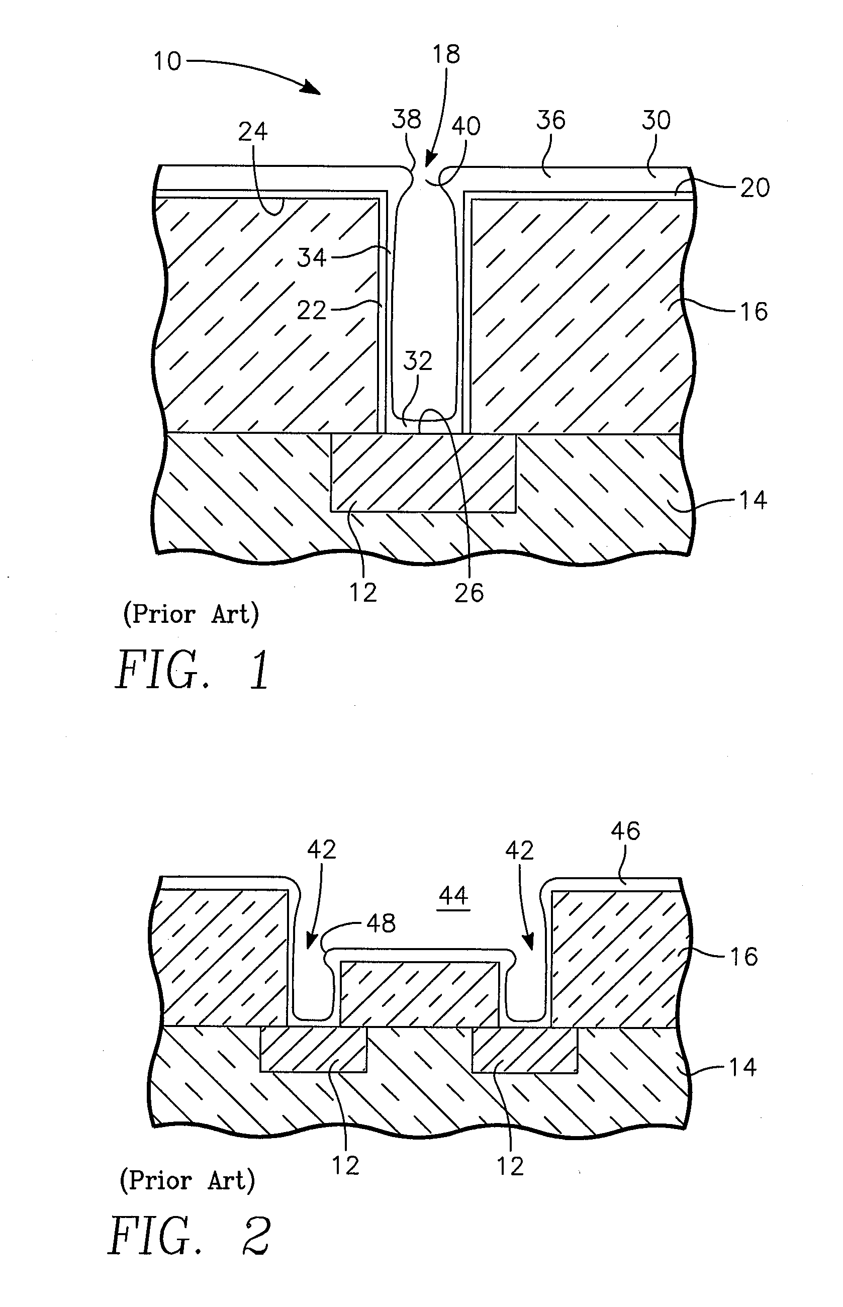
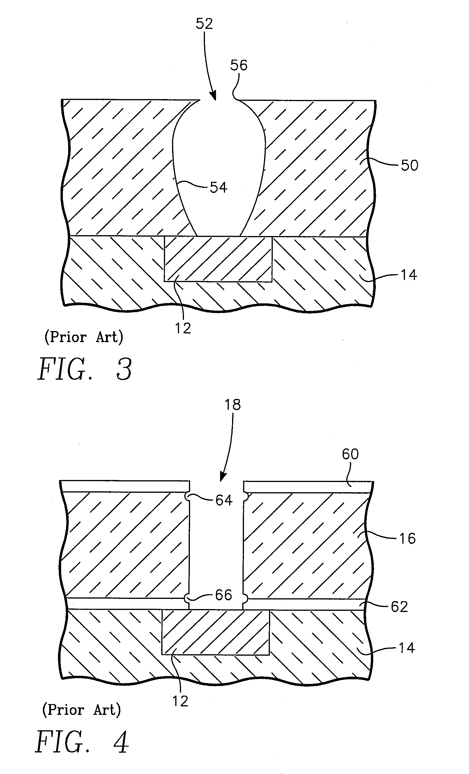
[0033]Filling copper into high aspect-ratio holes such as vias and dual-damascene interconnects is facilitated by a combination of copper sputter deposition and argon sputter etching preferably performed in a single copper sputter chamber. The energetic sputter etching reduces the size of overhangs and also tends to redistribute copper into concave portions of the sidewalls in a process often referred to as resputtering.

[0034]Although some aspects of the invention are not so limited, the sputter deposition and sputter etching are preferably performed in a chamber with an RF coil which can excite an argon plasma for the argon sputter etch with limited if any sputtering of the copper target during the etch phase. Ding et al. have described a sputter deposition / etch sequence of a tantalum barrier in an inductively coupled sputter chamber in U.S. patent application Ser. No. 10 / 915,139, filed Aug. 9, 2004, now published as U.S. patent application publication 2006 / 0030151. A similar sputt...


PUM

PropertyMeasurementUnit
thicknessaaaaaaaaaa
thicknessaaaaaaaaaa
aspect ratioaaaaaaaaaa

Abstract

An integrated copper deposition process, particularly useful for forming a copper seed layer in a narrow via prior to electrochemical plating of copper, including at least one cycle of sputter deposition of copper followed by sputter etching of the deposited copper, preferably performed in a same sputter chamber. The deposition is performed under conditions promoting high copper ionization fractions and strong wafer biasing to draw the copper ions into the via. The etching may be done with argon ions, preferably inductively excited by an RF coil around the chamber, or by copper ions, which may be formed with high target power and intense magnetron or by use of the RF coil. Two or more cycles of deposition/etch may be performed. A final flash deposition may be performed with high copper ionization and low wafer biasing.

Description

RELATED APPLICATION[0001]This application claims benefit of provisional application 60 / 888,893, filed Feb. 8, 2007.FIELD OF THE INVENTION[0002]The invention relates generally sputter deposition in the formation of semiconductor integrated circuits. In particular, the invention relates to a combination of sputter deposition and sputter etching in forming liner layers.BACKGROUND ART[0003]Magnetron sputtering has long been used in the deposition of horizontally extending layers of metallization such as aluminum and copper. More recently, magnetron sputtering has been adapted to the more challenging task of depositing liner layers in high aspect-ratio holes such as inter-level electrical contacts, also called vias. A via 10 for a copper metallization, illustrated in the cross-sectional view of FIG. 1, is formed over a conductive feature 12 at the surface of a lower dielectric layer 14. An upper dielectric layer 16 is deposited over the lower dielectric layer 14 and its conductive featur...

Claims


Application Information

Patent Timeline
Patent Type & Authority Applications(United States)
IPC IPC(8): C23C14/32
CPCC23C14/046C23C14/165C23C14/358C23C14/5826C23C14/584H01L21/76877H01J37/3455H01L21/2855H01L21/76865H01L21/76873H01J37/3408C23C14/35C23C14/22C23C14/14
Inventor TANG, XIANMINSUNDARRAJAN, ARVINDLUBBEN, DANIELLUO, QIANGUNG, TZA-JINGSUBRAMANI, ANANTHACHUNG, HUAFU, XINYUWANG, RONGJUNCAO, YONGYU, JICKFORSTER, JOHNGOPALRAJA, PRABURAM
Owner APPLIED MATERIALS INC
Why Eureka
Try Eureka