
Optical integrated circuit and manufacturing method therefor

a technology of optical integrated circuits and manufacturing methods, applied in the direction of optical elements, semiconductor lasers, instruments, etc., can solve the problems of limited silicon substrates on which a sio.sub.2 buffer layer can be formed by thermal oxidation, complex fabrication processes, and high cost, and achieve the effect of reducing waveguide loss

Inactive Publication Date: 2002-12-10
PIONEER CORP
View PDF7 Cites 3 Cited by
  • Summary
  • Abstract
  • Description
  • Claims
  • Application Information

AI Technical Summary

Benefits of technology

Accordingly, it is an object of the present invention to provide an optical integrated circuit which reduces a waveguide loss within a waveguide from an optical waveguide to a photodetector.
It is another object of the present invention to provide a method for manufacturing the above optical integrated circuit easily and at a low cost.

Problems solved by technology

In a structure or assembly that has a tapered optical coupling area, however, the substrate on which a SiO.sub.2 buffer layer can be formed by the thermal oxidation is limited to a silicon substrate.
Further, as the structure requires a process to be conducted under a vacuum condition and a high-temperature treatment, the fabrication process is complicated and the structure is expensive.
In a case where the optical coupling area takes a simple tapered structure, it is known that propagating light suffers a large optical loss at the curve portion of the optical waveguide layer.
To reduce the light loss, a scheme of controlling the taper angle has been considered, which, however, is difficult to achieve.
When a multi-layer structure is adopted, the process is originally complex.
Therefore, this structure is not suitable for detection of multi-wavelength signal light having different wavelengths to be detected.
To ensure efficient signal detection, the latter structure requires a relatively large photo-detection area as compared with the former structure that directly leads the waveguide layer to the photo-detection device, and is not therefore suitable for making the whole device, including the photo-detection device, compact.

Method used


Image

  • Optical integrated circuit and manufacturing method therefor
  • Optical integrated circuit and manufacturing method therefor
  • Optical integrated circuit and manufacturing method therefor

Examples


Embodiment Construction

The present invention will be described in detail as to one preferred embodiment of an optical integrated circuit produced by a method of the present invention, referring to the accompanying drawings.

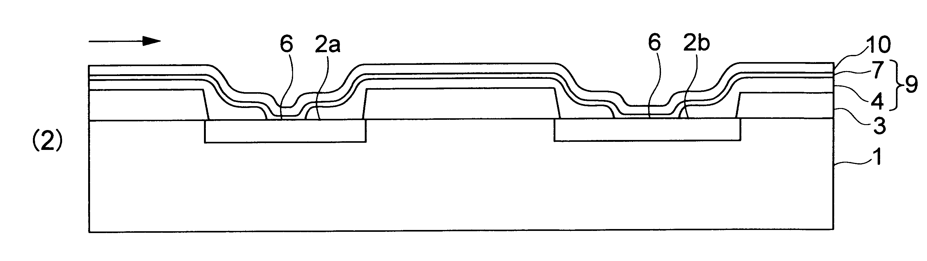
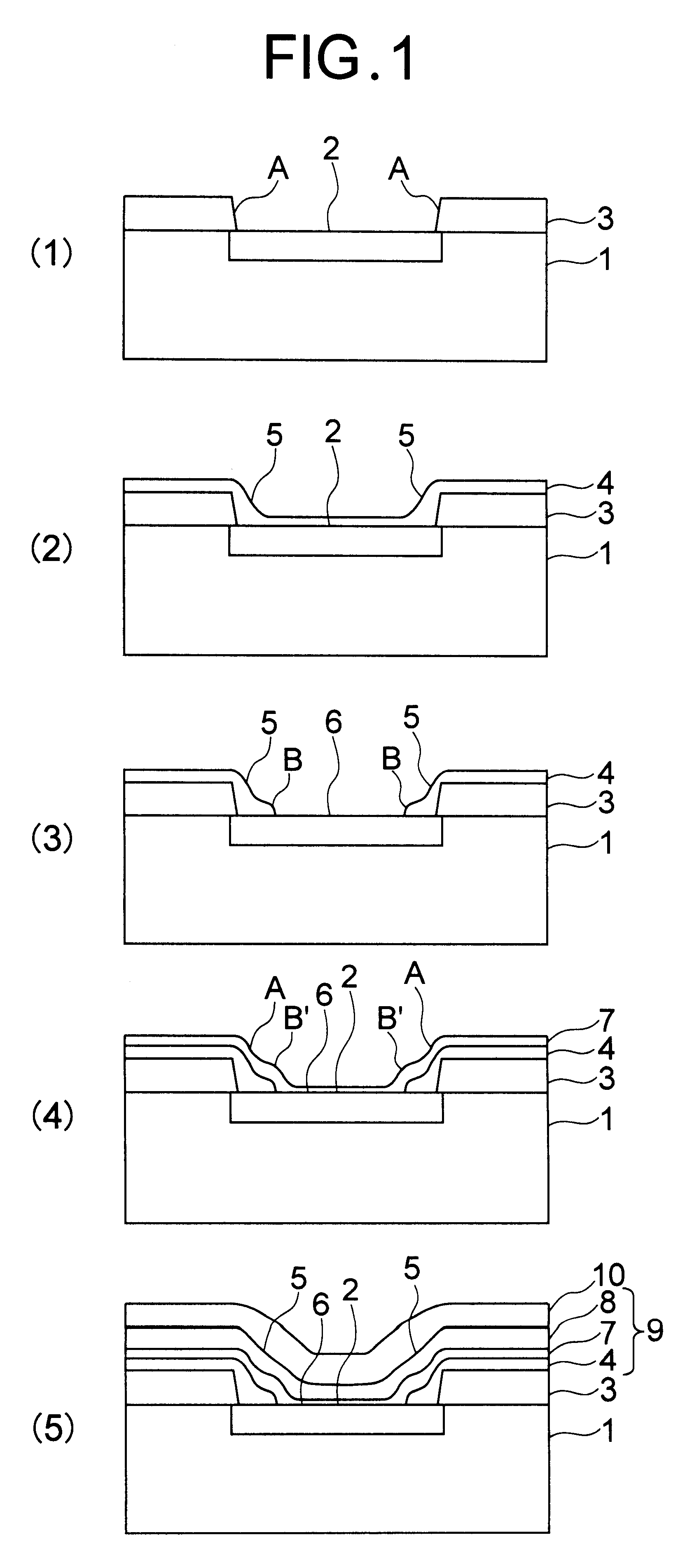
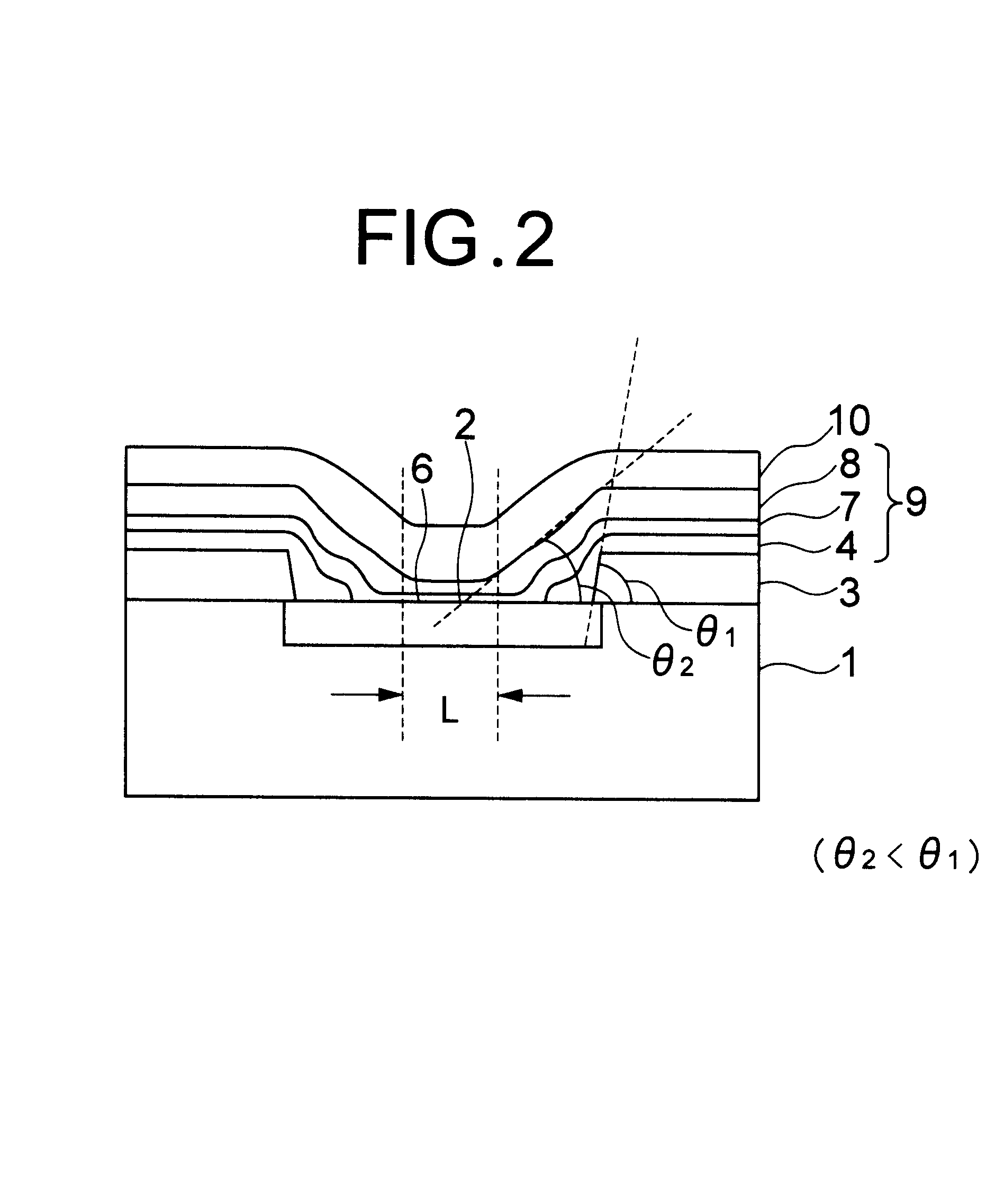
In FIG. 1, a photodetector 2 is formed as an optical device on one major surface of a silicon substrate 1 using a well-known process. Next, a light shielding layer 3 is formed of, for example, aluminum on one major surface of the substrate 1 excluding the area where the photodetector 2 is formed ((1) in FIG. 1). The light shielding layer 3 has a thickness sufficient to prevent stray light from above from reaching the substrate 1. The end face of the light shielding layer 3 is formed as a steep step portion A with respect to the photodetector 2.

Next, spin on glass (SOG) as a liquid insulator is spin-coated on the substrate 1 and cured, thereby forming a first sub-cladding layer 4 having a first refractive index n ((2) in FIG. 1). A curve portion 5 of the sub-cladding layer 4 formed on th...


PUM


Abstract

The present invention reduces the waveguide loss in an optical coupling between an optical waveguide layer and a photodetector. A cladding layer having a first refractive index is formed on a photodetector formed on a substrate by repeating spin-coating and curing of SOG. The cladding layer is formed in such a way as to gently cover a step portion between the photodetector and a light shielding layer. An optical waveguide layer which can allow propagating light to be coupled to the photodetector is formed on the cladding layer. This structure can suppress steep curvature of the optical waveguide layer above the photodetector.

Description

1. Technical FieldThe present invention relates to an optical integrated circuit and a manufacturing method thereof, and, more particularly, to an optical integrated circuit which couples light from an optical waveguide to a photodetector with a low loss and a method of manufacturing the structure.2. Related ArtA conventional waveguide optical signal detector comprises an SiO.sub.2 buffer layer formed on one major surface of, for example, a silicon substrate by thermal oxidation, a photodetector provided by an ordinary semiconductor process, a tapered optical coupling area formed on the photodetector by Local Oxidation of Silicon (LOCOS), and an optical waveguide layer formed thereon.In a case where the optical waveguide layer is of a phase matching type which takes a multi-layer structure, at least one optical waveguide layer other than the main optical waveguide layer and a cladding layer which is sandwiched between the optical waveguide layers are alternately deposited on the pho...

Claims


Application Information

Patent Timeline
Patent Type & Authority Patents(United States)
IPC IPC(8): G02B6/42G02B6/122G02B6/12H01L31/0232
CPCG02B6/12004G02B6/122G02B6/42G02B2006/12123
Inventor ONOE, ATSUSHI
Owner PIONEER CORP
Learn More