

El display device and electronic device
a display device and display device technology, applied in semiconductor devices, electrical devices, instruments, etc., can solve the problems of el driver tfts of pixels displaying colors with low light emission brightness degrading faster, and the brightness of red color images themselves which are displayed by the el display device is low
- Summary
- Abstract
- Description
- Claims
- Application Information
AI Technical Summary
Benefits of technology
Problems solved by technology
Method used
Image

Examples
embodiment 1
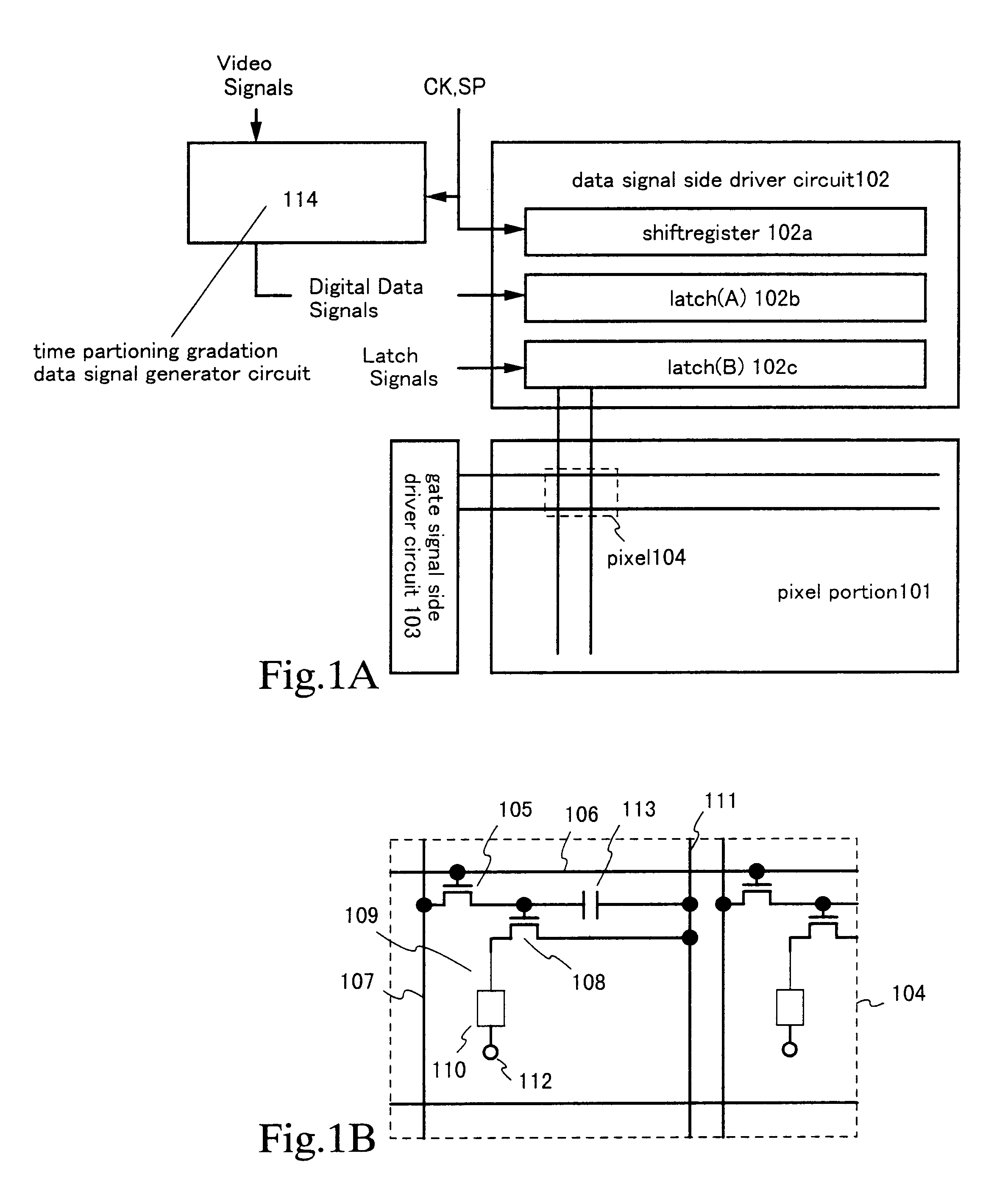
Time partitioning gradation display for a case of performing full color display of 256 gradations (16,770,000 colors) by an 8-bit digital driver method is explained in embodiment 1. Driving of an EL display device using an organic EL material in which the light emission brightness of the color red is less than the light emission brightnesses of the colors blue and green is explained in embodiment 1.
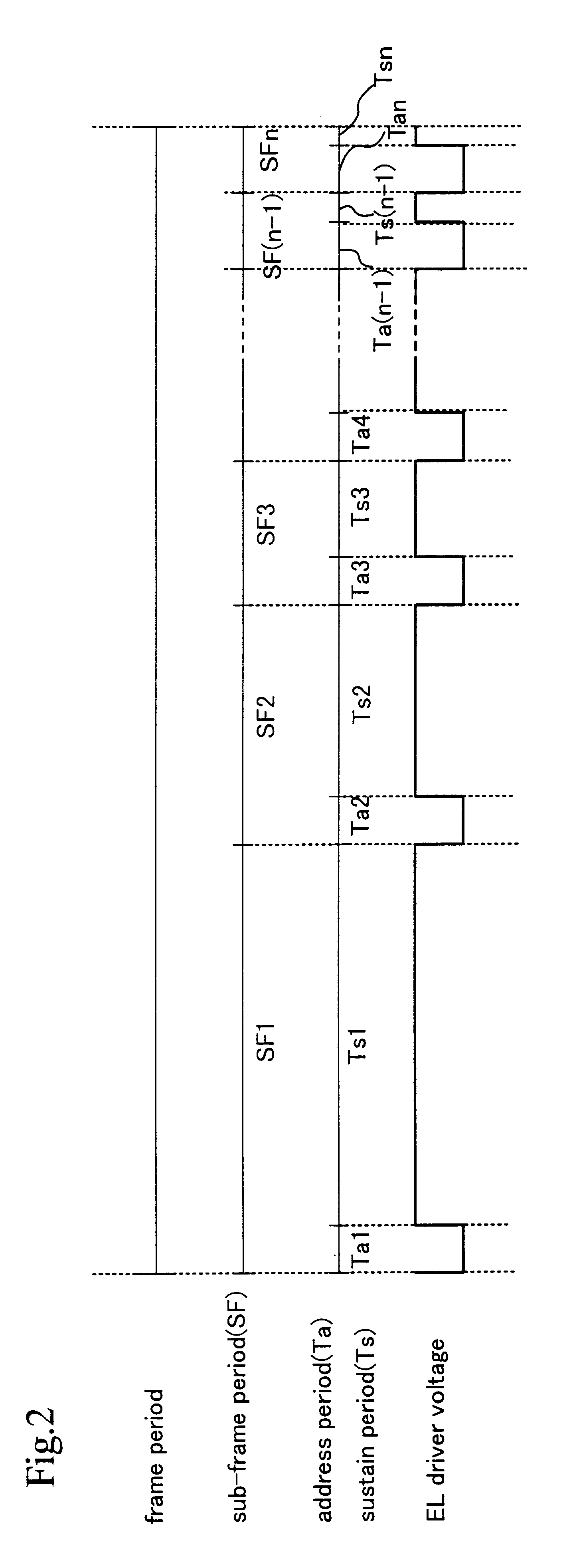
First, one frame period is partitioned into 8 sub-frame periods (SF1 to SF8). The emission frequency is set at 60 Hz in the EL display device of embodiment 1, 60 frame periods are formed in one second, and 60 images are displayed in one second. (See FIG. 3.)
One sub-frame period is divided into an address period (Ta) and a sustain period (Ts). The lengths of the address periods (Ta1 to Ta8) of SF1 to SF8 are respectively all fixed. The sustain periods (Ts) of SF1 to SF8 are referred to as Ts1 to Ts8, respectively.
The length of the sustain periods is set so as to become Ts1: Ts2: Ts3: Ts4: ...
embodiment 2
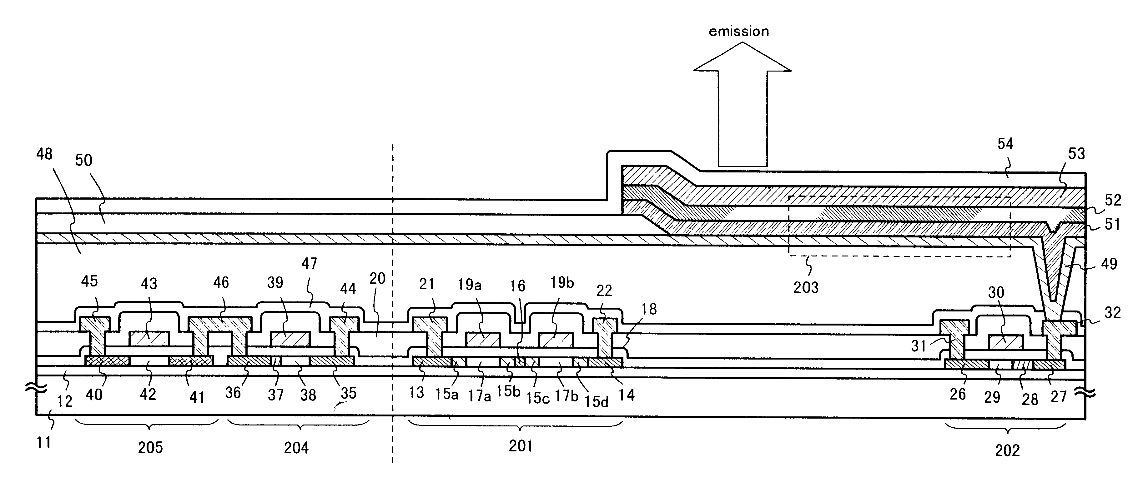
Next, reference is made to FIG. 4 schematically showing the sectional structure of the EL display device of the present invention. This embodiment explains the example of a cathode of an EL element connected to the drain region of the EL driver TFT.
In FIG. 4, reference numeral 11 is a substrate, and 12 is an insulating film that is a base (hereinafter, this film is designated as base film). For the substrate 11, use can be made of a light transmissible substrate, representatively, a glass substrate, a quartz substrate, a glass ceramic substrate, or a crystallization glass substrate. However, it must be resistible to the highest processing temperature in a manufacturing process.
The base film 12 is effective especially in using a substrate that contains a movable ion or a substrate that has conductivity, but it is not necessarily disposed on the quartz substrate. An insulating film that contains silicon can be used as the base film 12. It should be noted that, in this specification, "...
embodiment 3
In this embodiment, a description is here given of a method of simultaneously manufacturing TFTs of a pixel portion and a driving circuit portion around the pixel portion. Concerning the driving circuit, a CMOS circuit that is a base unit is shown in the figure, for a brief description.
First, a substrate 501 in which a base film (not shown) is disposed on the surface thereof is prepared as shown in FIG. 5(A). In this embodiment, a silicon nitride oxide film whose thickness is 200 nm and another silicon nitride oxide film whose thickness is 100 nm are laminated and are used as a base film on a crystallization glass. At this time, preferably, the concentration of nitrogen of the film contacting the crystallization glass substrate is kept to 10-25 wt %. It is possible to form an element directly on the quartz substrate without any base film, of course.
Thereafter, an amorphous silicon film 502 whose thickness is 45 nm is formed on the substrate 501 by a well-known film formation method....
PUM
 Abstract
Description
Claims
Application Information