Timing difference division circuit and signal controlling method and apparatus

a division circuit and signal control technology, applied in the direction of pulse manipulation, pulse technique, computation using pulse rate multipliers/dividers, etc., can solve the problem of insufficient operating speed, achieve the effect of increasing chip area, preventing the increase of chip area, and increasing operating speed

Inactive Publication Date: 2003-04-08
RENESAS ELECTRONICS CORP
View PDF12 Cites 19 Cited by
  • Summary
  • Abstract
  • Description
  • Claims
  • Application Information

AI Technical Summary

Benefits of technology

In the structure of the conventional timing difference division circuit, shown in, for example, FIG. 26 etc., the MOS transistors and the MOS capacitance are used to adjust the value of the capacitance of the capacitance device CAP appended to the inner node, there is required an area corresponding to the area of the MOS transistors and the MOS capacitances, thus increasing the chip area.
It is therefore an object of the present invention to provide a timing difference division circuit and a method for timing difference division whereby the operating speed may be increased and the chip area may be prevented from being increased while enabling a broadband operation.

Problems solved by technology

On the other hand, the PLL circuit, shown in FIG. 25, has a drawback that it is insufficient in operating speed, since clocks obtained on frequency division of the output of the VCO 322 will be of a frequency equal to the frequency of the external clock 324, such that a time interval not less than several tens of clock periods must elapse until the clocks multiplied in frequency are obtained.

Method used


Image

  • Timing difference division circuit and signal controlling method and apparatus
  • Timing difference division circuit and signal controlling method and apparatus
  • Timing difference division circuit and signal controlling method and apparatus

Examples


Embodiment Construction

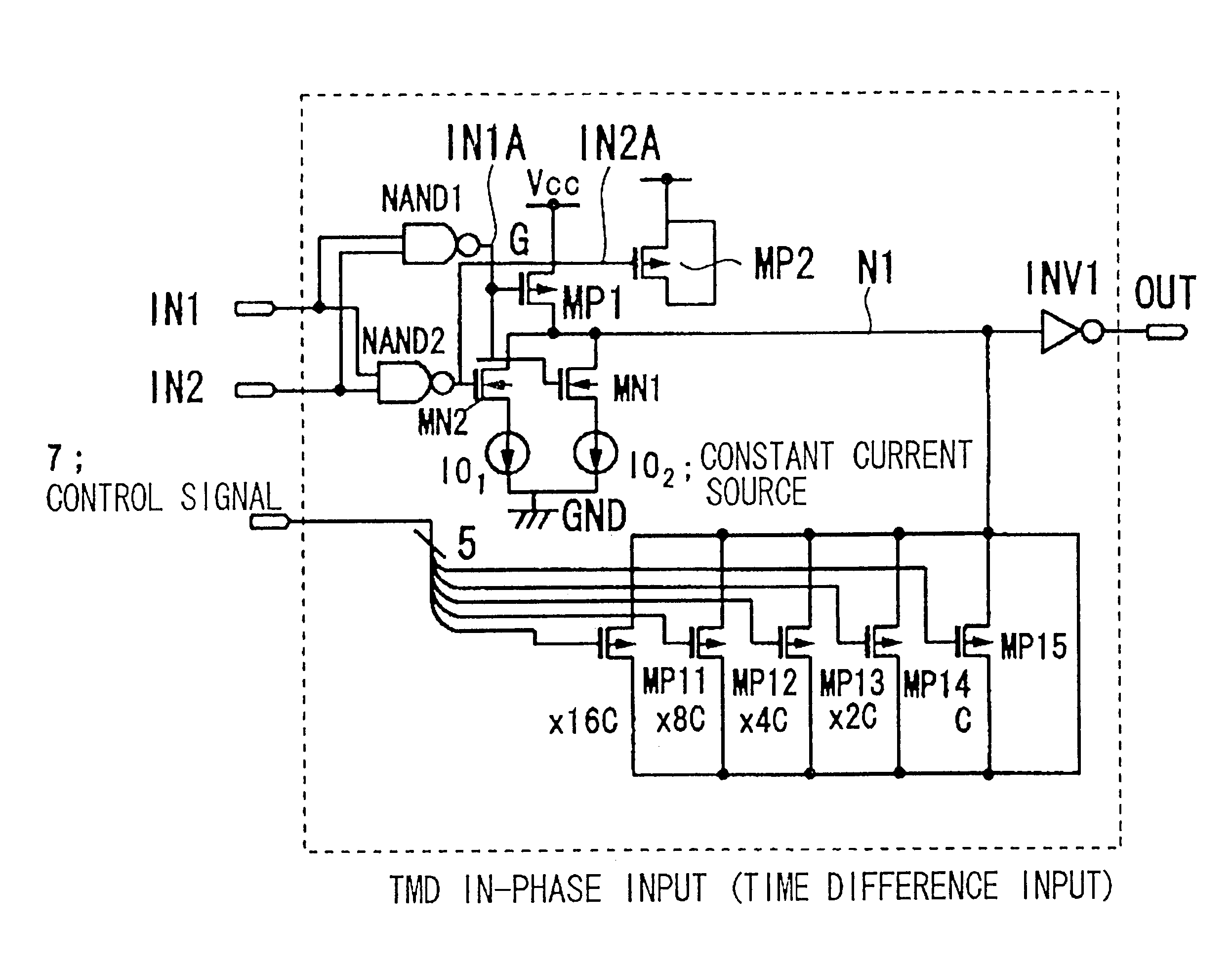
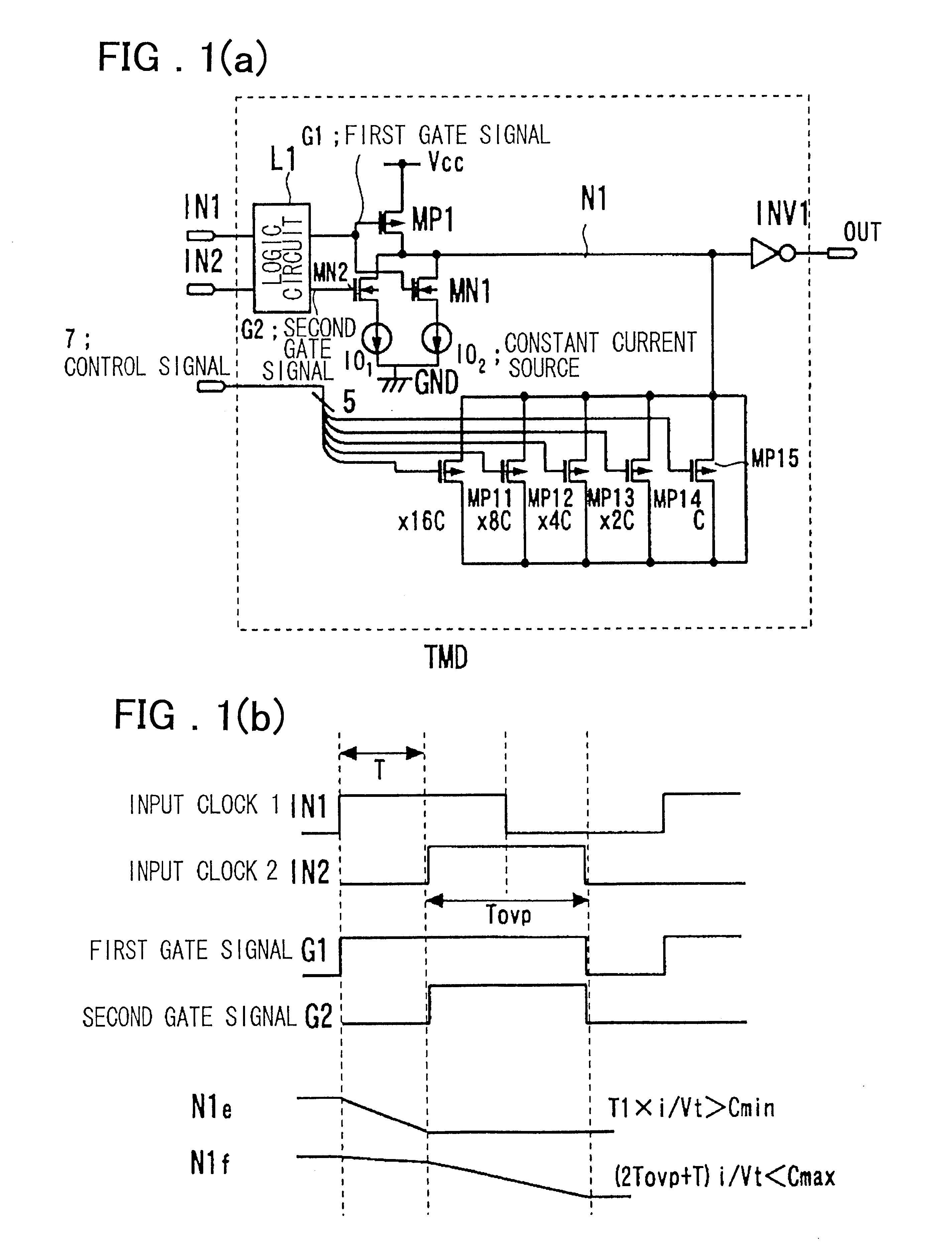
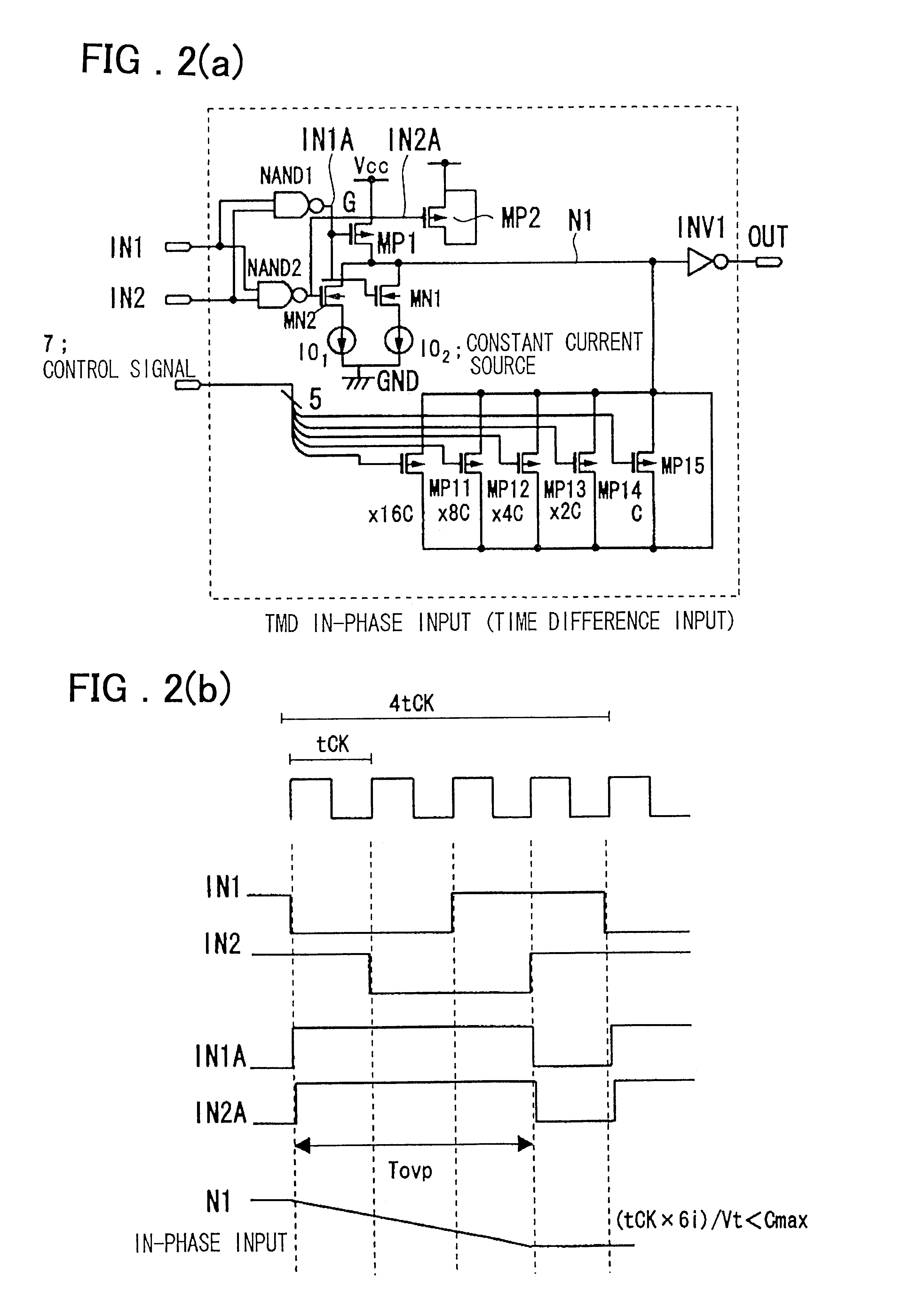
An embodiment of the present invention is explained. The present invention is directed to a timing difference division circuit at least including two switches MN1, MN2 connected in parallel to control a path between an inner node N1 and a power source on or off, one of the switches MN1 being turned on based on one of two input signals IN1, IN2 undergoing faster transition to charge or discharge a capacitance C appended (connected) to the inner node N1 with a first current (I), the other switch MN2 being turned on based on the other input signal undergoing transition with a delay with respect to the one input signal, the capacitance appended to the inner node being charged or discharged through the one switch in the on-state and the other switch in the on-state with a current value corresponding to a sum (2I) of the first current and a second current; there being provided a buffer circuit INV1 an output logic value of which is changed when the voltage of the inner node exceeds or is ...


PUM


Abstract

Timing difference division circuit with a high operating speed and a small area, assuring broadband operation. The circuit includes a logic circuit L1 generating a first gate signal and a second gate signal based on a first input signal and a second input signal, a first switch element connected across a first power source and an inner node and having a control terminal to which is fed the first gate signal, a first series circuit made up of a second switch element and a first constant current source and a second series circuit made up of a third switch element and a second constant current source. The first and second series circuits are connected in parallel across the inner node and the second power source. The first and second gate signals are connected to control terminals of the second and third switches, respectively. The circuit also includes a plurality of MOS capacitors, connection of which to the inner node is separately controlled by a control signal, and a buffer circuit an input end of which is connected to the inner node and the value of an output signal of which is determined based on the relative magnitude of the potential of the inner node and a threshold voltage. An overlap period during which the first and second gate signals output from the logic circuit are both activated to turn on the second and third switch elements is set to an optional value.

Description

This invention relates to a signal controlling method and apparatus.A conventional signal dividing method for dividing (internally dividing or interpolating) a timing difference is used for multiplying the frequency of clock signals, as disclosed in Publication 1 (Japanese patent application 09-157028 (JP Patent Kokai JP-A-11-4145)).In e.g., Publication 2 (ISSCC Digest of Technical Papers pp.216 to 217, February 1996, U.S. Pat. Nos. 5,442,835 and 5,530,837), there is disclosed a clock signal frequency multiplying circuit, as shown herein in FIG. 24.Referring to FIG. 24, the clock signal frequency multiplying circuit is made up of four sets of delay circuits 301 to 304, a phase comparator 309 and a counter 310, in case of 4.times. frequency multiplying.Each of the first to fourth delay circuits 301 to 304 has its output terminals selected by first to fourth switchers 305 to 308, with the first to fourth delay circuits 301 to 304 being connected in series with one another.A first cloc...

Claims


Application Information

Patent Timeline
Patent Type & Authority Patents(United States)
IPC IPC(8): H03K5/00H03K5/13G06F7/68
CPCG06F7/68H03K5/00006H03K5/133H03K2005/00071H03K2005/00065H03K5/00
Inventor SAEKI, TAKANORI
Owner RENESAS ELECTRONICS CORP
Why Eureka
Try Eureka