Process for fabricating a self-aligned vertical bipolar transistor

Inactive Publication Date: 2003-04-22
STMICROELECTRONICS SRL
View PDF11 Cites 21 Cited by
  • Summary
  • Abstract
  • Description
  • Claims
  • Application Information

AI Technical Summary

Benefits of technology

The sacrificial layer may be made of polysilicon, or else of silicon-germanium, thereby making it easier to remove the sacrificial layer.
The sacrificial layer is preferably removed by isotropic plasma etching, using a gas mixture consisting of hyd

Problems solved by technology

Yet, another shortcoming leads to degradation of the high-frequency performance of these transistors

Method used


Image

  • Process for fabricating a self-aligned vertical bipolar transistor
  • Process for fabricating a self-aligned vertical bipolar transistor
  • Process for fabricating a self-aligned vertical bipolar transistor

Examples


Embodiment Construction

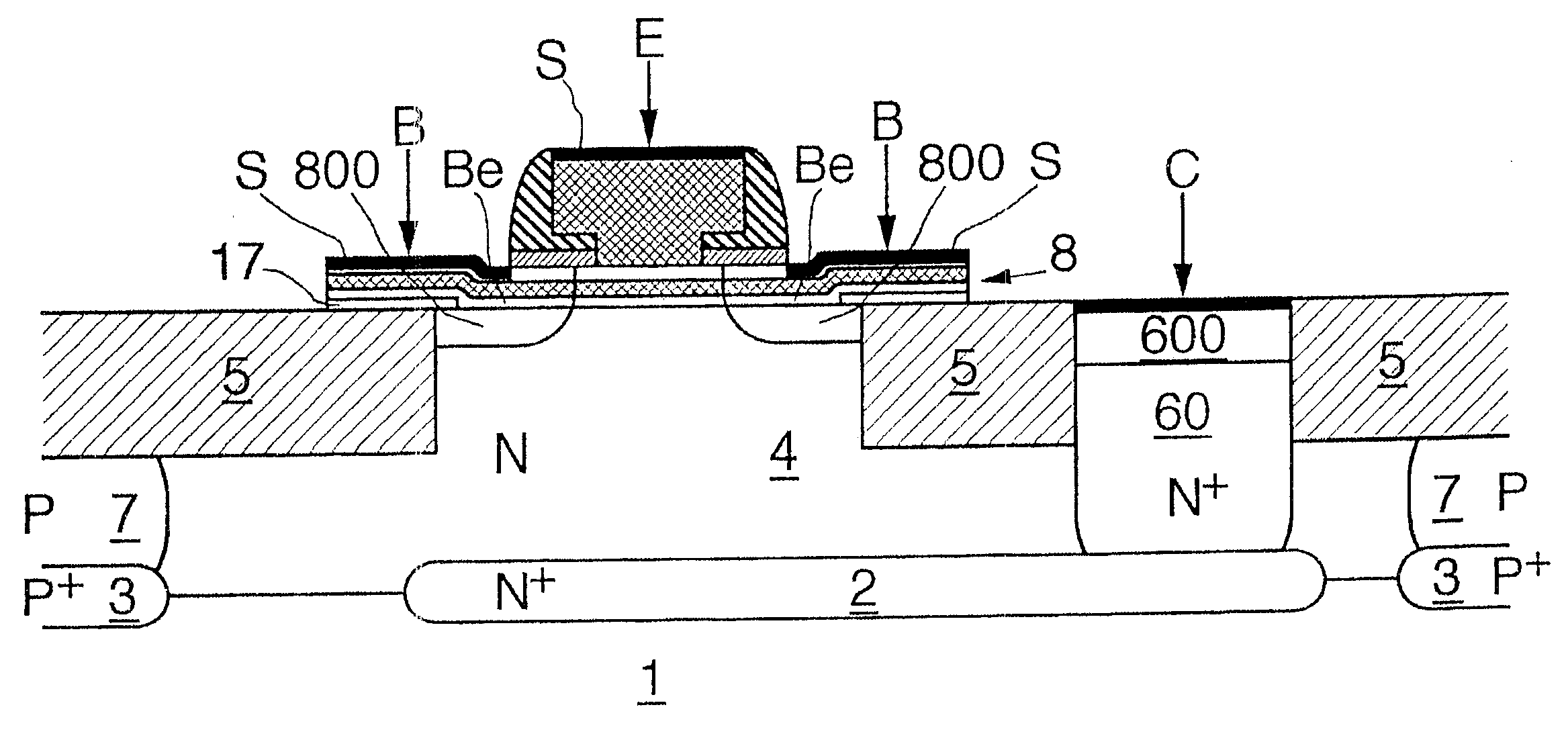
In FIG. 1, the reference number 1 denotes a silicon substrate, for example a p-type silicon substrate, on the surface of which an n.sup.+ -doped buried extrinsic collector layer 2 has been conventionally produced, in a known manner, by arsenic implantation.

Likewise, two p.sup.+ -doped buried layers 3 are conventionally produced, on either side of the extrinsic collector 2, by boron implantation.

Thick epitaxy is carried out, in a manner known per se, on the substrate 1 thus formed so as to produce a layer 4 of n-type monocrystalline silicon having a thickness typically of the order of 1 micron.

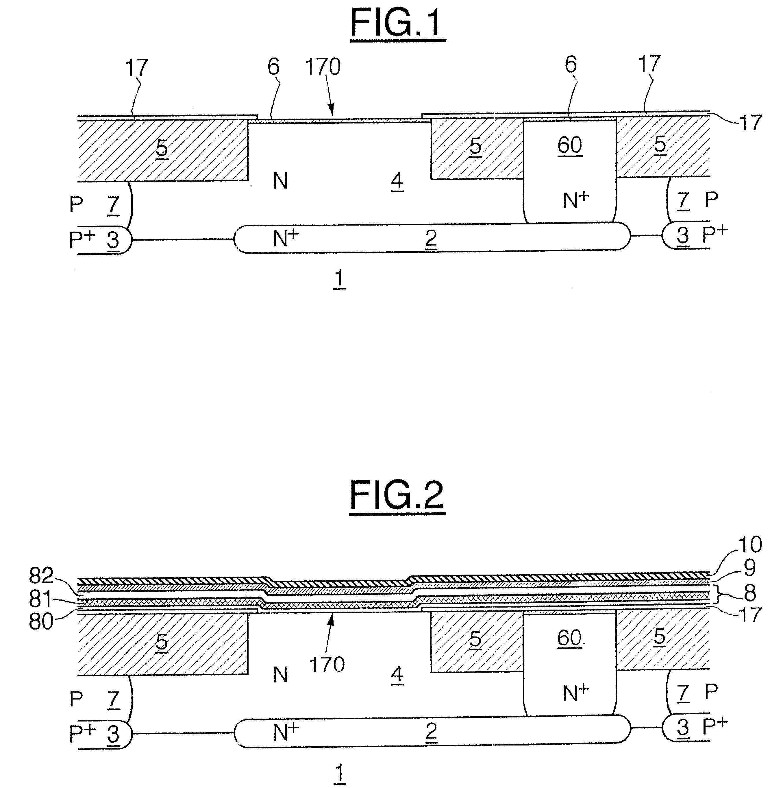
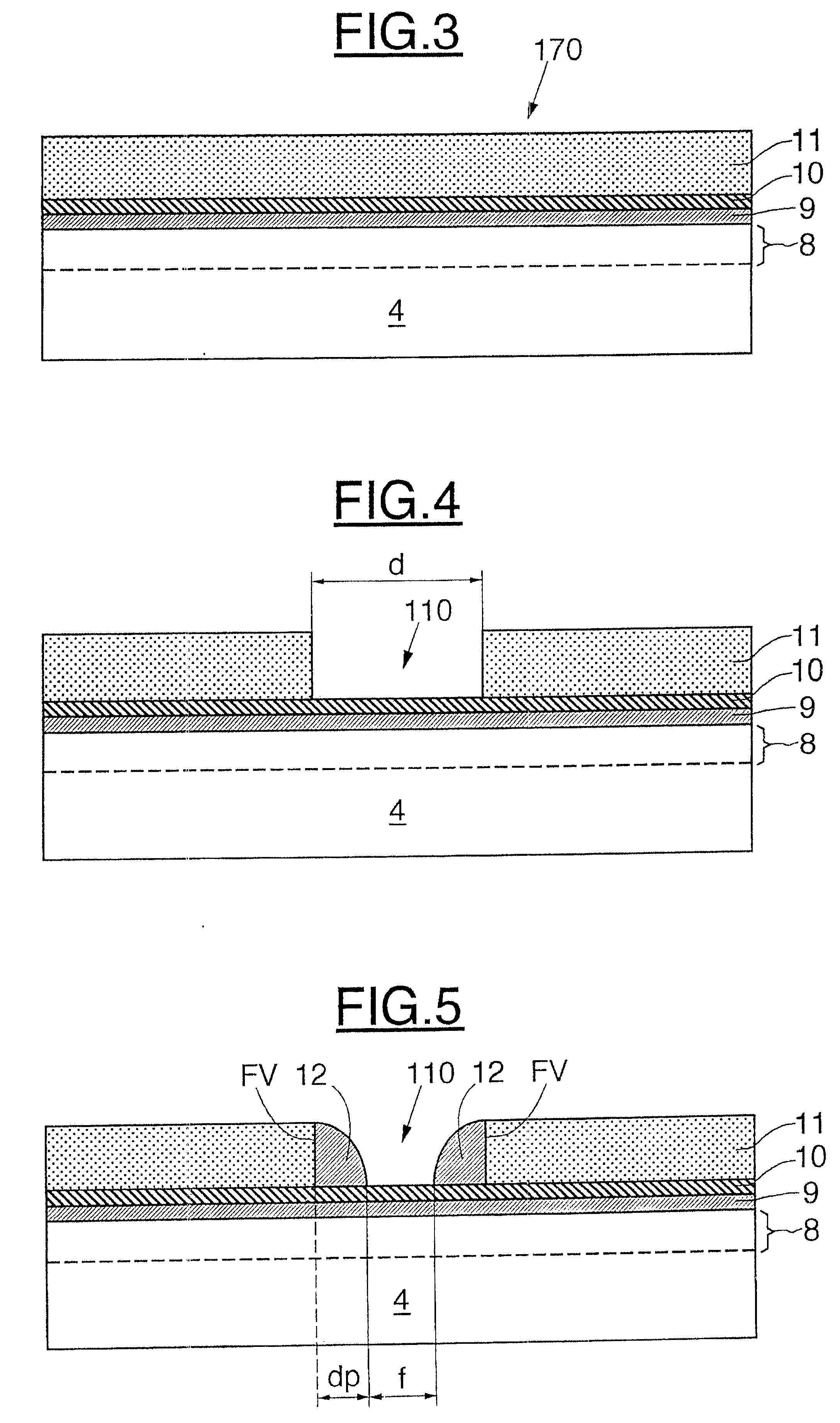
Next, a lateral isolating region 5 is produced in this layer 4, in a manner known per se, by either a localized oxidation process (or LOCOS) or a process of the "shallow trench" type.

A lateral isolating region 5 of the shallow-trench type has been shown in FIG. 1 for the sake of simplification.

Also produced conventionally, especially by phosphorus implantation, is an n.sup.+ -doped collector we...


PUM


Abstract

The fabrication process comprises a phase of producing a base region having an extrinsic base and an intrinsic base, and a phase of producing an emitter region comprising an emitter block having a narrower lower part located in an emitter window provided above the intrinsic base. Production of the extrinsic base comprises implantation of dopants, carried out after the emitter window has been defined, on either side of and at a predetermined distance dp from the lateral boundaries of the emitter window, so as to be self-aligned with respect to this emitter window, and before the emitter block is formed.

Description

This application is based upon and claims priority from prior French Patent Application No. 9911895, filed Sep. 23, 1999, the entire disclosure of which is herein incorporated by reference.1. Field of the InventionThe present invention relates to vertical bipolar transistors, especially those intended to be integrated into high-frequency very-large-scale integrated technologies (VLSI), and in particular to the production of the extrinsic base and of the emitter window of these transistors.2. Description of Related ArtIn polysilicon-emitter bipolar technologies, the emitter region generally comprises an emitter block having a narrower lower part located in a window, called the "emitter window", provided above the intrinsic base of the transistor. The emitter block also has a wider upper part which extends beyond the emitter window and rests on an insulating layer (generally formed from two insulating sublayers) above the base region.Implantation of the extrinsic base takes place on e...

Claims


Application Information

Patent Timeline
IPC IPC(8): H01L21/331H01L21/02H01L29/73H01L21/205H01L21/302H01L21/3065H01L29/737
CPCH01L29/66272H01L29/66242
Inventor CHANTRE, ALAINMARTY, MICHELBAUDRY, HELENE
Owner STMICROELECTRONICS SRL
Why Eureka
Try Eureka