

Hetero-junction field effect transistor having an intermediate layer
a junction field and transistor technology, applied in the direction of basic electric elements, electrical appliances, semiconductor devices, etc., can solve the problems of power loss, power gain decrease, power delivering efficiency for a large signal amplitude decrease,
- Summary
- Abstract
- Description
- Claims
- Application Information
AI Technical Summary
Benefits of technology
Problems solved by technology
Method used
Image

Examples
first embodiment
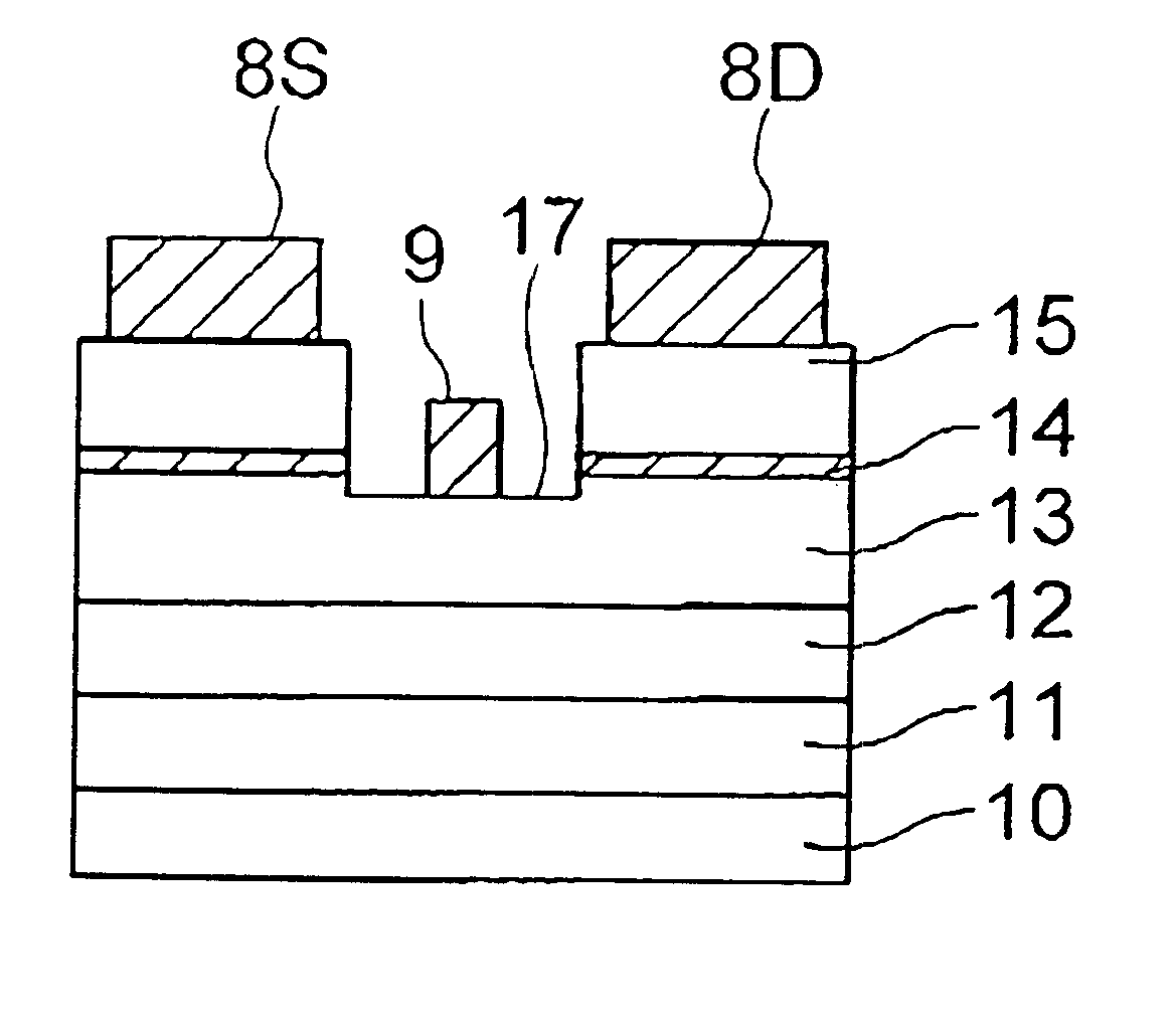
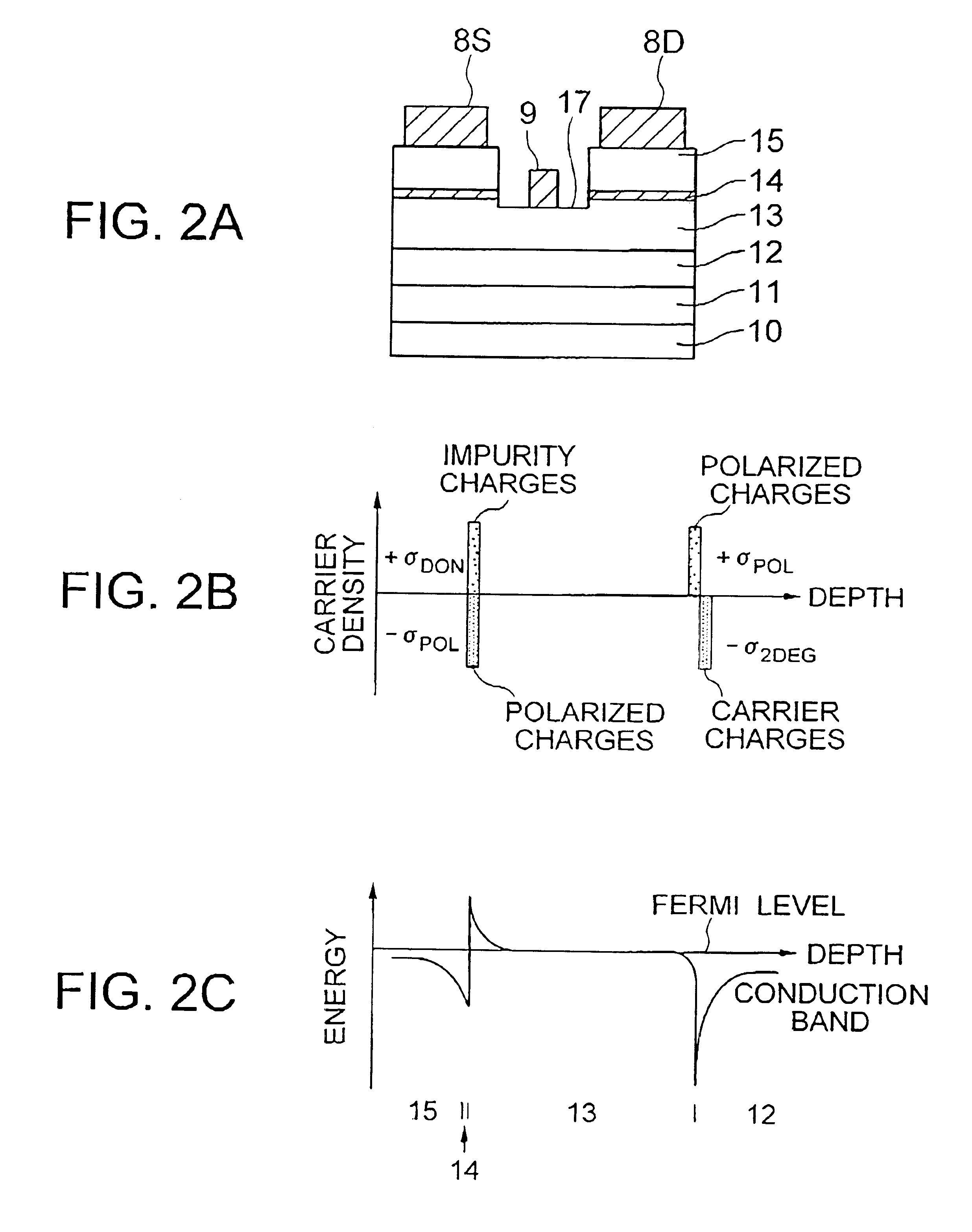
FIG. 2A schematically shows the structure of a HJFET according to a first embodiment of the present invention in a cross section thereof. The HJFET has an undoped aluminum nitride (AlN) buffer layer 11, an undoped GaN channel layer 12, an n-type AlGaN electron supply layer 13, an Si monoatomic layer 14 and an n-type GaN cap layer 15 which are stacked sequentially on a sapphire substrate 10.
The Si monoatomic layer 14 constitutes an intermediate layer. Two-dimensional electron gas is generated in the vicinity of the interface between the GaN channel layer 12 and the AlGaN electron supply layer 13. A source electrode 8S and a drain electrode 8D are formed on the n-type GaN cap layer 15 while making an ohmic contact therewith. A gate electrode 9 is formed on the n-type AlGaN electron supply layer 13 while making a Schottky contact therewith, in a recess 17 which is formed by removing part of the semiconductor layers 15, 14, 13.
In the HJFET of this embodiment, the source electrode 8S and...
second embodiment
FIG. 3A schematically shows the HJFET of this embodiment. The HJFET has an undoped GaN buffer layer 21, an n-type GaN channel layer (n-type impurity concentration 5.times.10.sup.17 / cm.sup.3, film thickness 30 nm) 22, an undoped Al.sub.0.2 Ga.sub.0.8 N electron supply layer (film thickness 30 nm) 23, an n-type Al.sub.0.2 Ga.sub.0.8 N layer (n-type impurity concentration 1.times.10.sup.19 / cm.sup.3, film thickness 10 nm) 24 and an n-type GaN cap layer (n-type impurity concentration 5.times.10.sup.18 / cm.sup.3, film thickness 50 nm) 25 which are stacked sequentially on a silicon carbide (SiC) substrate 20.
The n-type Al.sub.0.2 Ga.sub.0.8 N layer 24 constitutes an intermediate layer While AlGaN and GaN have different lattice constants, the total thickness 40 nm of the Al.sub.0.2 Ga.sub.0.8 N layers (23, 24) is below the critical thickness for the occurrence of dislocation. Two-dimensional electron gas is generated in the vicinity of the interface between the GaN channel layer 22 and th...
third embodiment
FIG. 4A schematically shows the HJFET of this embodiment. The HJFET has an undoped AlN buffer layer 31, an undoped GaN channel layer 32, an n-type Al.sub.0.2 Ga.sub.0.8 N electron supply layer (n-type impurity concentration 2.times.10.sup.18 / cm.sup.3, film thickness 30 nm) 33, an Si monoatomic layer (surface density of n-type impurity 5.5.times.10.sup.12 / cm.sup.2) 34a, an undoped Al.sub.0.1 Ga.sub.0.9 N layer (film thickness 5 nm) 34b, an Si monoatomic layer (surface density of n-type impurity 5.5.times.10.sup.12 / cm.sup.2) 34c and an n-type GaN cap layer (n-type impurity concentration 5.times.10.sup.18 / cm.sup.3, film thickness 50 nm) 35 which are stacked sequentially on a sapphire substrate 30.
The Si monoatomic layer 34a, the undoped Al.sub.0.1 Ga.sub.0.9 N layer 34b and the Si monoatomic layer 34c constitute an intermediate layer. While AlGaN and GaN have different lattice constants, the total thickness 35 nm of the AlGaN layers (33, 34b) is below the critical thickness for the...
PUM
 Abstract
Description
Claims
Application Information