Method of improving gate activation by employing atomic oxygen enhanced oxidation

a technology of atomic oxygen and enhanced oxidation, which is applied in the direction of semiconductor devices, electrical equipment, transistors, etc., can solve the problems of poor transistor reliability and severe poly depletion problems in small devices, and achieve the effects of reducing the thermal budget of the sidewall oxidation process, reducing the cost of oxidation, and minimizing the poly depletion

Inactive Publication Date: 2003-05-20
IBM CORP
View PDF2 Cites 37 Cited by
  • Summary
  • Abstract
  • Description
  • Claims
  • Application Information

AI Technical Summary

Benefits of technology

A further object of the present invention is to provide a method of fabricating a Si-based MIS transistor in which the thermal budget of the sidewall oxidation process is significantly reduced so as to maintain the small grain sizes within the gate conductor.
A yet further object of the present invention is to provide a method of fabricating a Sibased MIS transistor which minimizes the poly depletion effects that are typically observed in prior art Si-based MIS transistors.
An even further object of the present invention is to provide a method of fabricating a Si-based MIS transistor which prevents the grains of the gate conductor from getting larger by reducing the thermal budget of the sidewall oxidation process utilizing a process which is easy to implement with existing technologies.
These and other objects and advantages are achieved in the present invention by utilizing atomic oxygen as the oxidative ambient during the sidewall gate oxidation step. The use of atomic oxygen during sidewall oxidation has unexpectedly reduced the thermal budget of the oxidation process by a factor of one or two orders of magnitude as compared with typical thermal budgets obtained by prior art sidewall oxidations. The lowering of the thermal budget of the sidewall oxidation process results in the formation of a Si-based MIS transistor comprising a Si-containing semiconductor polycrystalline gate conductor whose grain sizes are about 0.1, preferably 0.05, .mu.m or less.

Problems solved by technology

A higher comer electric field can produce large hot-carrier effects leading to poor transistor reliability.
This can prevent dopants reaching the bottom interface and can cause severe poly depletion problems in small devices.

Method used


Image

  • Method of improving gate activation by employing atomic oxygen enhanced oxidation
  • Method of improving gate activation by employing atomic oxygen enhanced oxidation
  • Method of improving gate activation by employing atomic oxygen enhanced oxidation

Examples


Embodiment Construction

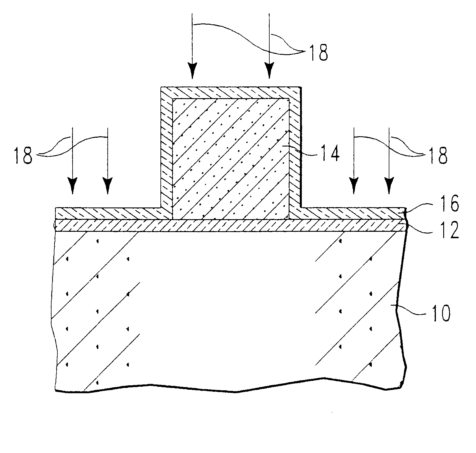
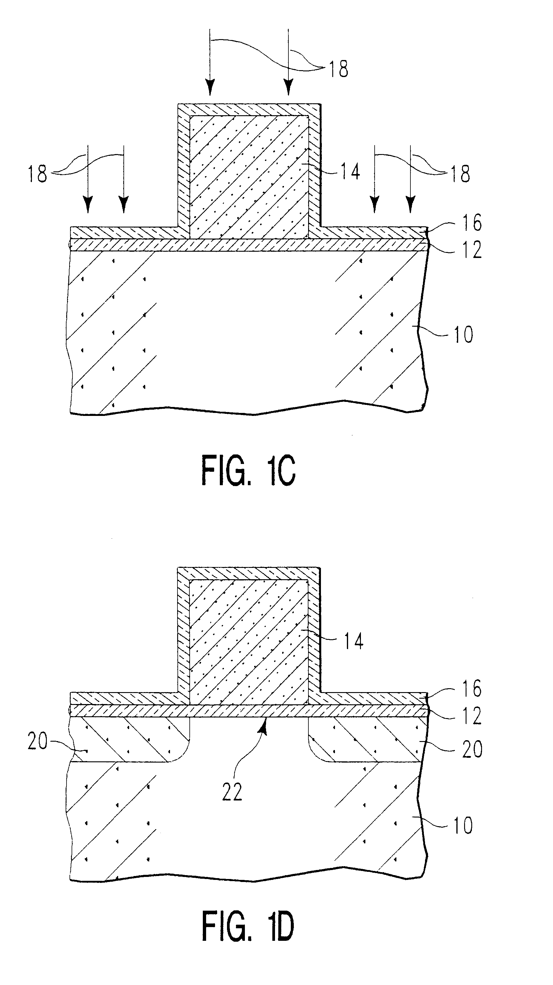
The present invention, which provides a method for preventing the polycrystalline grains of a Si-containing gate conductor from getting larger, by reducing the thermal budget of the sidewall oxidation process, will now be described in more detail by referring to the drawings that accompany the present invention. It is noted that in the accompanying drawings like and / or corresponding elements are referred to by like reference numerals.

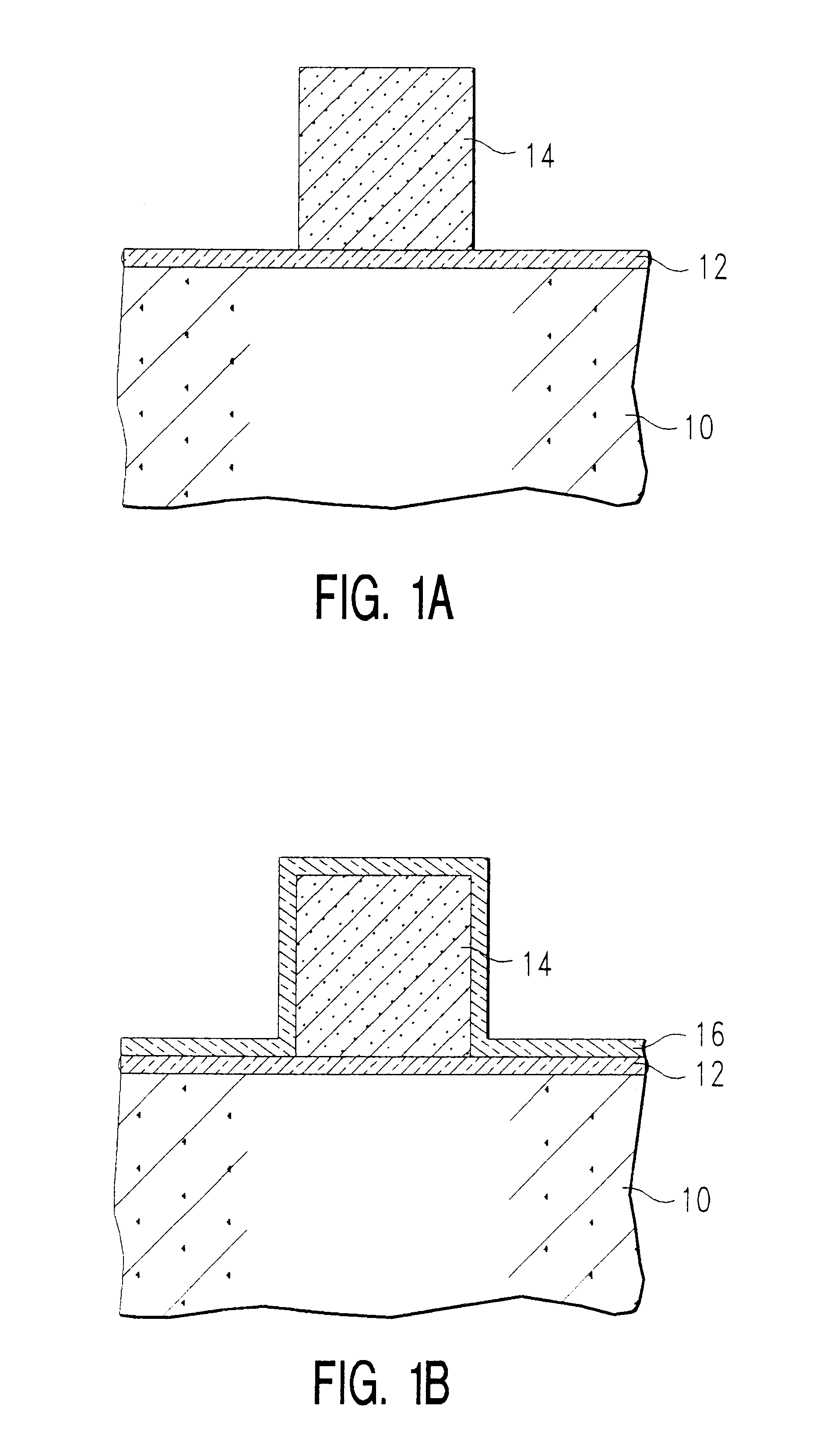
Reference is first made to FIG. 1A which illustrates an initial structure that can be employed in the present invention. Specifically, the initial structure shown in FIG. 1A comprises Si-containing substrate 10, gate dielectric 12, and patterned region of Si-containing semiconductor polycrystalline material 14. Although only one patterned region of Si-containing semiconductor polycrystalline material is shown in the drawings, the present invention works equally well when more than one patterned region of Si-containing semiconductor polycrystalline mater...


PUM


Abstract

The present invention provides a method of preparing a Si-based metal-insulator-semiconductor (MIS) transistor which prevents the polycrystalline grains of the gate conductor from getting significantly larger by reducing the thermal budget of the sidewall oxidation process. The thermal budget of the inventive sidewall oxidation process is reduced one or two orders of magnitude over conventional prior art sidewall oxidation processes by utilizing atomic oxygen as the oxidizing ambient. The present invention also provides Si-based MIS transistors having a gate conductor having grain sizes of about 0.1, preferably 0.05, .mu.m or less.

Description

FIELD OF THE INVENTIONThe present invention relates to semiconductor device fabrication, and more particularly to a method of fabricating Si-based metal-insulator-semiconductor (MIS) transistors comprising at least a Si-containing semiconductor polycrystalline gate conductor, e.g., polysilicon, SiGe, or SiGeC, wherein the gate conductor has grain sizes of about 0.1 .mu.m or less.BACKGROUND OF THE INVENTIONModem Si-based metal-insulator-semiconductor (MIS) field effect transistors (FETs) containing polysilicon gate conductors are typically fabricated with the use of socalled sidewall or comer oxidation of the gate comer. Sidewall oxidation processes are routinely employed in conventional process flows such as complementary metal oxide semiconductor (CMOS) logic, static random access memory (SRAM), dynamic random access memory (DRAM), embedded DRAM, flash memories and other like processing flows.As is known to those skilled in the art, sidewall oxidation of the gate comers thickens th...

Claims


Application Information

Patent Timeline
Patent Type & Authority Patents(United States)
IPC IPC(8): H01L21/02H01L21/28H01L29/49H01L21/321H01L29/40H01L21/316H01L29/423H01L29/78H01L29/786
CPCH01L21/28035H01L29/4916H01L21/32105H01L21/8234
Inventor AJMERA, ATUL C.DOKUMACI, OMER H.DORIS, BRUCE B.GLUSCHENKOV, OLEG
Owner IBM CORP
Why Eureka
Try Eureka