

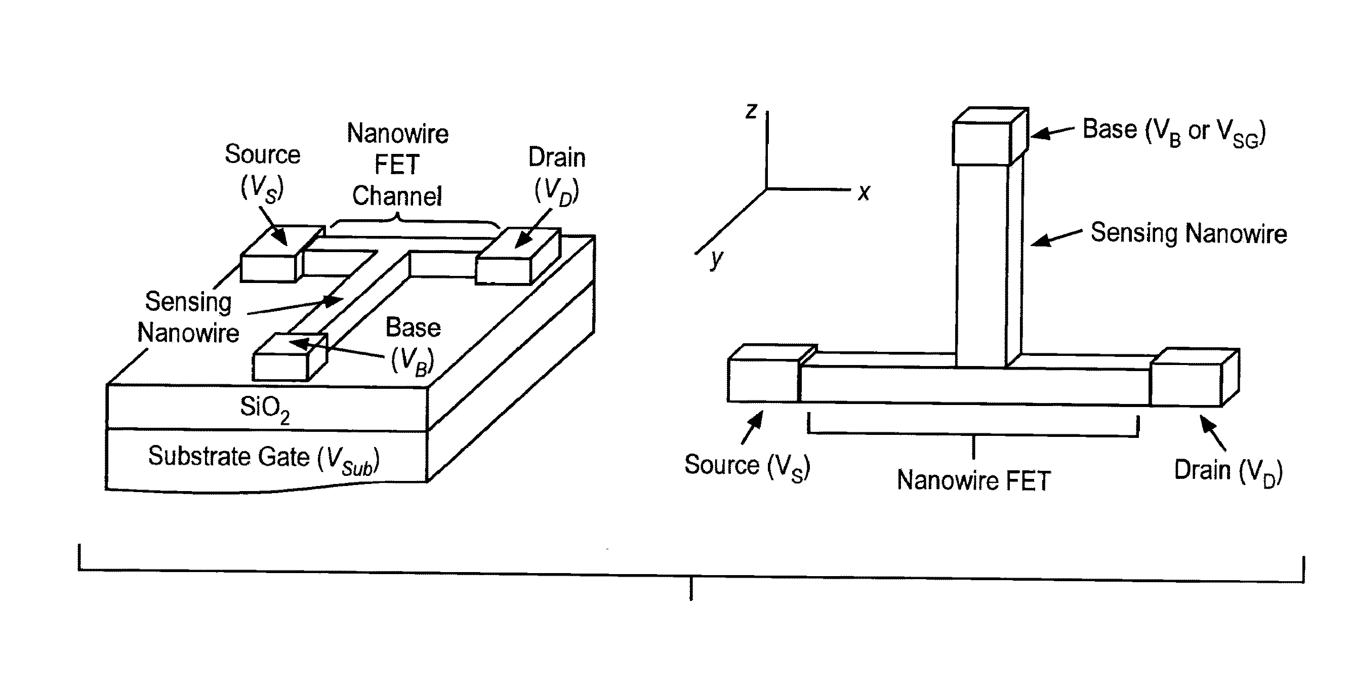
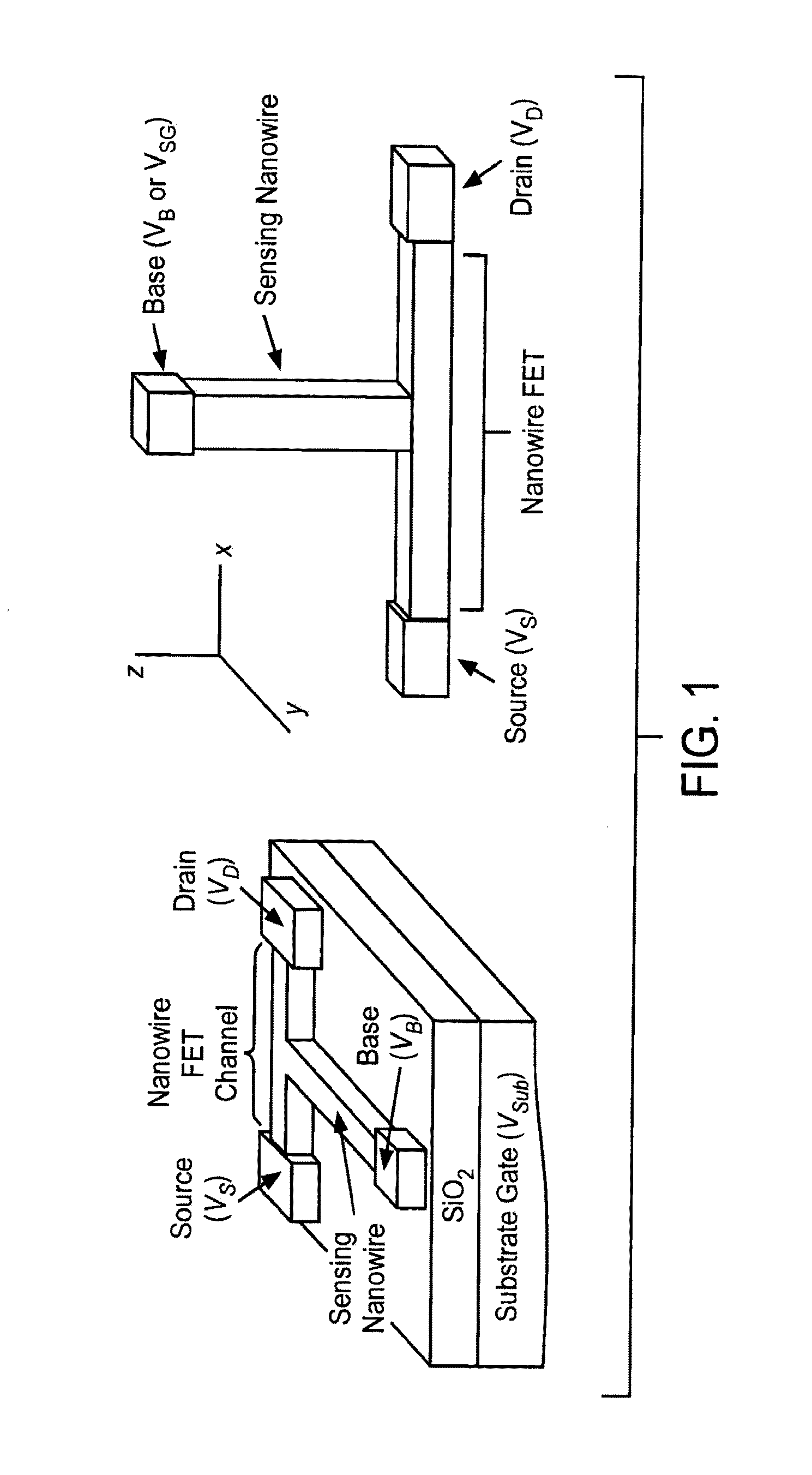
Nanowire field-effect transistor biosensor with improved sensitivity
a field-effect transistor and biosensor technology, applied in nanosensors, instruments, material analysis, etc., can solve the problems of low output signal and hinder and achieve the effect of good sensitivity, low output signal and hindering the ultimate performance of the devi
- Summary
- Abstract
- Description
- Claims
- Application Information
AI Technical Summary
Benefits of technology
Problems solved by technology
Method used
Image

Examples
example 1
Si T-nwFET Device Characterization
[0140]DC characteristics of the nwFET channel were measured. The device included a 10 μm long and 100 nm wide sensing nanowire and nanowire FET channel.
[0141]Results showed an inverse sub-threshold slope S ˜294 mV / decade at 0.2 V drain voltage (FIG. 11). Additionally, the gate voltage-drain current transfer characteristics were shifted to the left with an increased drain voltage (FIG. 11, top). Without wishing to be bound by theory, the shift was thought to be due to the reduction of the Schottky barrier by the drain potential similar to the dram-induced barrier lowering (DIBL) effect in a MOSFET. Thus, a higher minimum drain current in the off-state was obtained.
[0142]When the base electrode (i.e., the sensing nanowire) was floated, the output characteristics across the source and drain electrodes with a varying substrate gate voltage, VSub (inset in FIG. 11, bottom left), resembled those of a conventional Schottky nwFET. These data verified the ba...
example 2
pH Sensing Measurements with the Si T-nwFET Compared to a Conventional Si nwFET
[0147]T-channel devices used in these studies were fabricated as described above. SEM images of the conventional nanowire and T-channel nanowire device are provided in FIG. 14.
[0148]In order to detect hydrogen ion concentration (or pH), the sensing Si nanowire surface was first functionalized with 3-aminopropyltriethoxysilane (APTES) molecules to form exposed amino groups (—NH2) (FIG. 6). These groups act as receptors of hydrogen ions that undergo the protonation or deprotonation reactions. An increase in the ambient pH increases the negative charge density on the nanowire surface and thus changes the nanowire conductance.
[0149]During the actual sensing operation, the VSG bias was fixed such that an ambient pH variation on the SG surface directly changed its conductance and thus ISG. The potential at the middle node was then modulated. This in turn resulted in the Schottky barrier height and / or width modu...
example 3
Bulk Sensing Performance of the T-nwFET
[0154]The bulk sensing performance of the novel T-nwFET was examined against that of the cofabricated Schottky I-nwFET (i.e., single channel nanowire) in this study. The detection of the probe station microscope light was chosen for the study with the assumption that the light intensity would stay constant throughout. While the entire I-nwFET was unshielded, only the sensing nanowire in T-nwFET was exposed by shadowing the source and drain nanowire channels and Schottky contacts with a Teflon mold. The light was turned off initially for about 1.5 s and then turned on, and biasing voltages were applied to the devices under test for 0.6 s duration in each lighting condition.
[0155]Real-time measurements of ID (for I-nwFET), and IB and ID (for T-nwFET) were taken as shown in FIG. 15. The I-nwFET ID level with light was higher than in dark because the incident light reduces the nanowire resistance at fixed VD and VS. The T-nwFET IB and ID levels exh...
PUM
| Property | Measurement | Unit |
|---|---|---|
| angle | aaaaa | aaaaa |
| angle | aaaaa | aaaaa |
| width | aaaaa | aaaaa |
Abstract
Description
Claims
Application Information