High dielectric constant materials forming components of DRAM storage cells

a technology of dielectric constant materials and dram storage cells, which is applied in the direction of semiconductor devices, electrical equipment, capacitors, etc., can solve the problems of limited high-k dielectric used in drams, limited dram performance that is determined by the drivability of mos devices, and limited k dielectric us

Inactive Publication Date: 2002-08-27
IBM CORP
View PDF4 Cites 29 Cited by
  • Summary
  • Abstract
  • Description
  • Claims
  • Application Information

AI Technical Summary

Problems solved by technology

Further, the high-k dielectric used in DRAMs is limited (mostly) by the material stability as well as the topography.
The resulting non-planar surface has created problems for metallization as well as lithographic patterning.
On the other hand, the performance of the DRAM that is determined by the drivability of MOS device is also now limited by the scaling.
As the channel width and oxide thickness of the devices cannot be reduced, the device performance begins to degrade.
This becomes worse, when the Vdd (the power supply) level is also reduced.
Eventually, if DRAM cost cannot be reduced, the system of using large-volume DRAM will become expensive.
This reduces the process cost, and also reduces the thermal budget seen while annealing the dielectric.

Method used


Image

  • High dielectric constant materials forming components of DRAM storage cells
  • High dielectric constant materials forming components of DRAM storage cells
  • High dielectric constant materials forming components of DRAM storage cells

Examples


Embodiment Construction

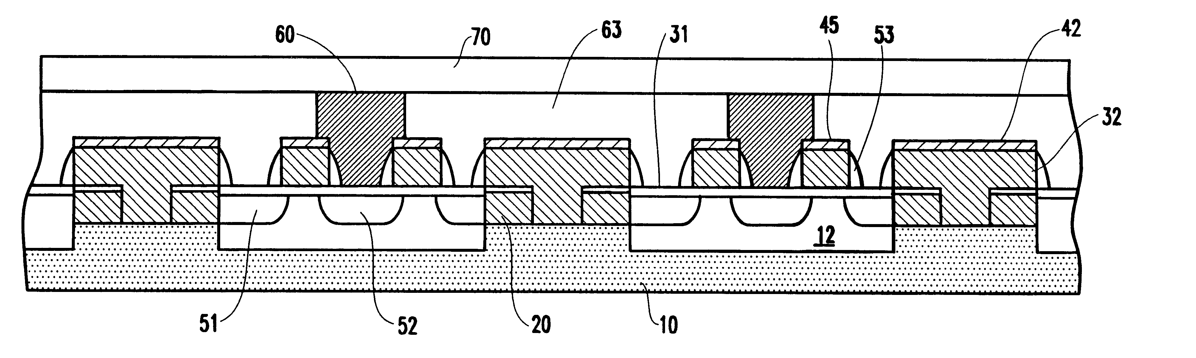
As mentioned above, there is a need to reduce the cost and improve performance of DRAM. The invention addresses these needs by providing a high-k material for both device gate dielectrics as well as capacitor dielectrics in a DRAM device. In a preferred embodiment, the invention uses a high-k film made using atomic level chemical vapor deposition (ALCVD) techniques. Using ALCVD to deposit a combination of La.sub.2 O.sub.3 / Al.sub.2 O.sub.3 obtains a dielectric constant between 10 and 30 depending on the ratio of Al to La. The invention uses deposition conditions that retain the amorphous nature of the film stack in order to prevent electrical leakage. Details of the material characteristic and associated process steps to form such material is reported by Albert Chin, et al, in 2000 Symposium of VLSI Technology Digest of Technical Papers, pp 16-17, titled "High Quality La2O3 and Al2O3 Gate Dielectrics with Equivalent Oxide Thickness 5-10 A".

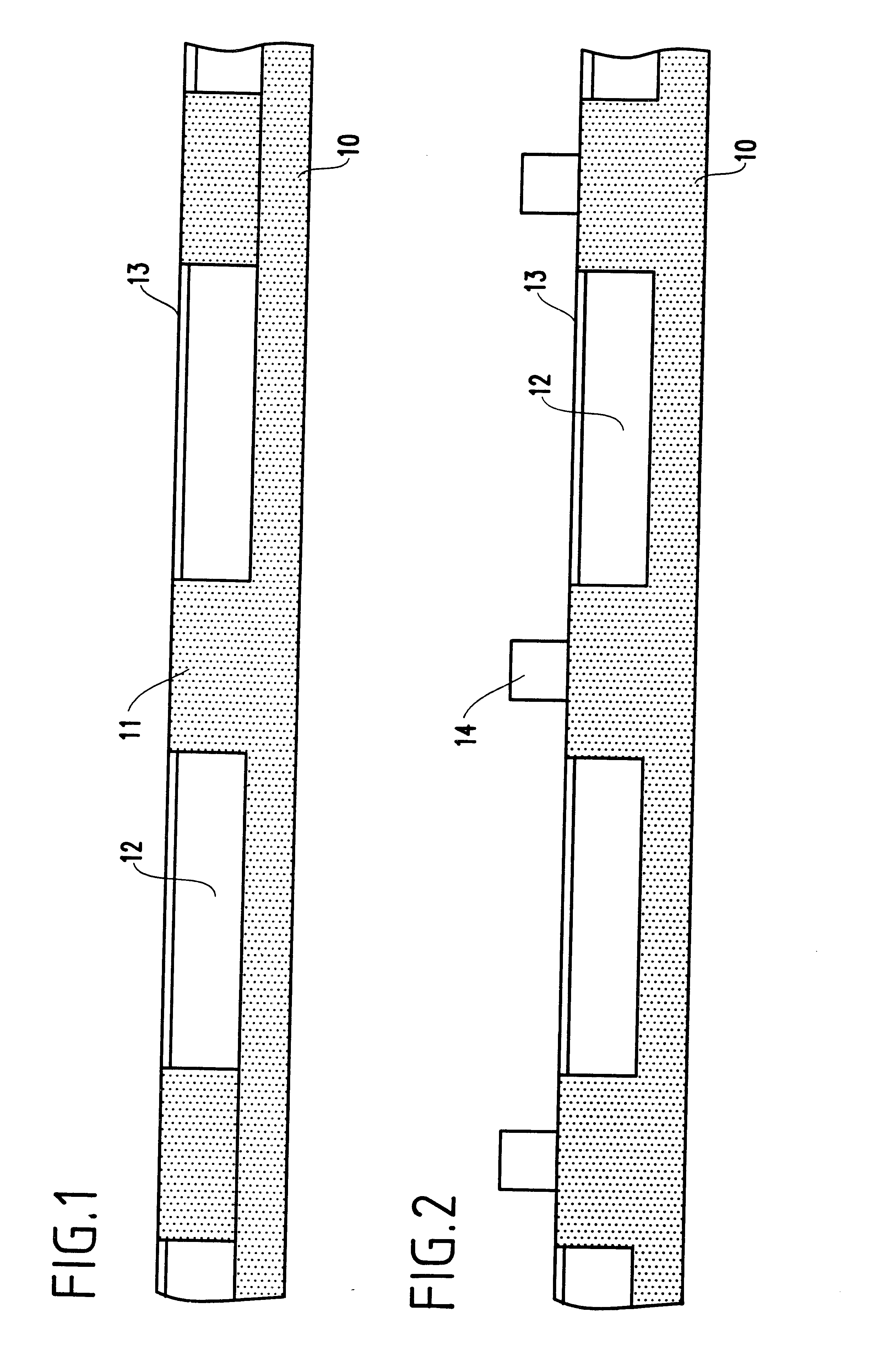
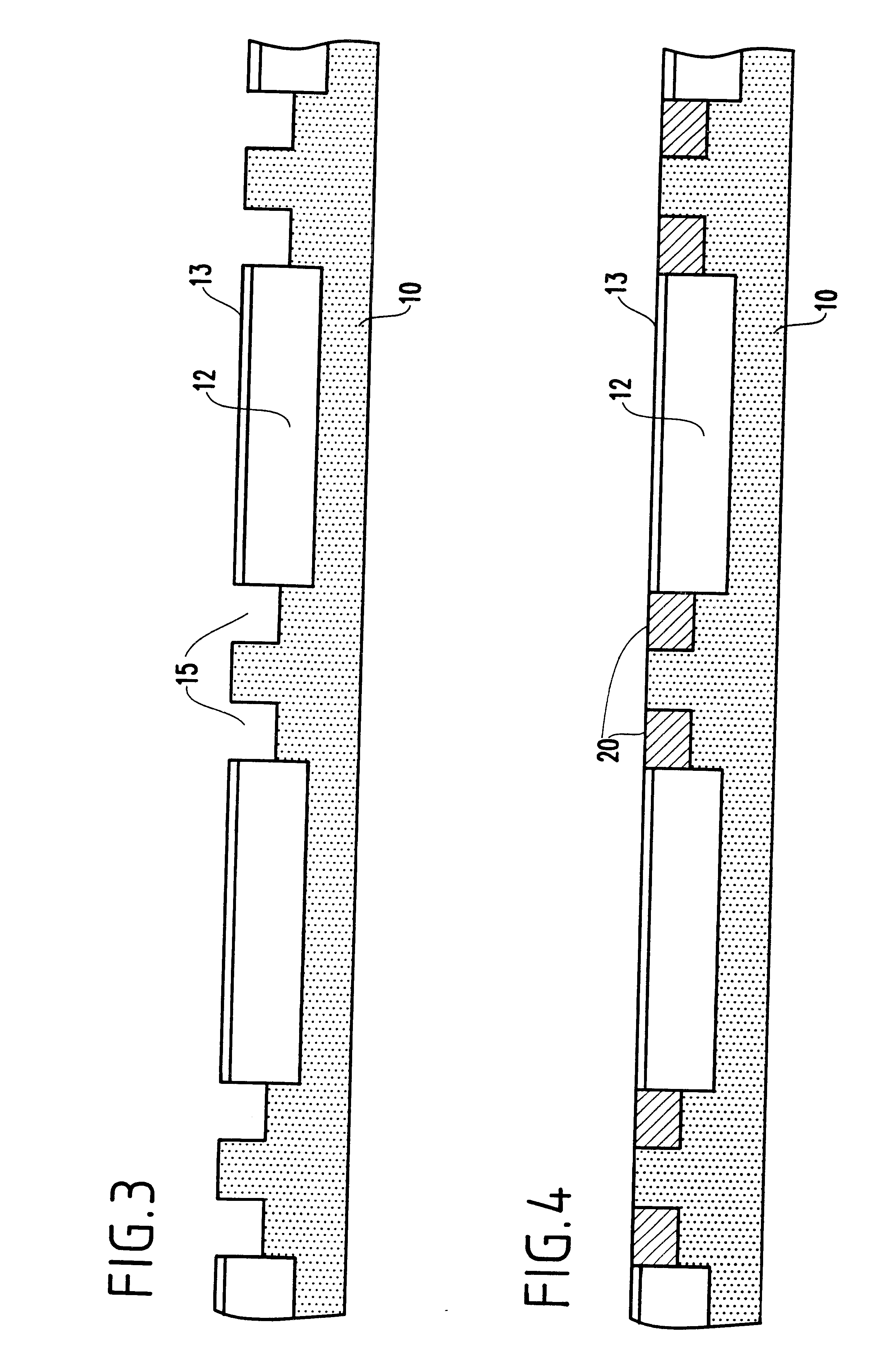
The invention forms high-k dielectrics in a...


PUM


Abstract

A method and structure for simultaneously producing a dynamic random access memory device and associated transistor is disclosed. The method forms channel regions and capacitor openings in a substrate. Next, the invention deposits capacitor conductors in the capacitor openings. Then, the invention simultaneously forms a single insulator layer above the channel region and above the capacitor conductor. This single insulator layer comprises a capacitor node dielectric above the capacitor conductor and comprises a gate dielectric above the channel region.

Description

1. Field of the InventionThe present invention generally relates to integrated storage devices and more particularly to an improved dynamic random access memory dielectric structure.2. Description of the Related ArtDynamic random access memory (DRAM), is known to have a much higher memory density than static random access memory (SRAM) for the same chip area. To achieve high DRAM integration, either deep trench-capacitor or high-k dielectric stack-capacitor cells are commonly used. The deep trench capacitor has a planar surface topography, although the depth of the trench has become the limiting factor to prevent the scaling of DRAM exceeding 4Gb. Further, the high-k dielectric used in DRAMs is limited (mostly) by the material stability as well as the topography. The stack-capacitor is built on top of the silicon surface. The resulting non-planar surface has created problems for metallization as well as lithographic patterning. On the other hand, the performance of the DRAM that is ...

Claims


Application Information

Patent Timeline
Patent Type & Authority Patents(United States)
IPC IPC(8): H01L21/70H01L21/8242H01L21/02H01L27/12H01L27/108H01L29/786
CPCH01L27/1085H01L27/10861H01L27/10867H01L27/10873H01L27/1203H01L28/55H10B12/03H10B12/038H10B12/0385H10B12/05
Inventor CLEVENGER, LAWRENCE A.HSU, LOUIS L.RADENS, CARL J.SHEPARD, JR., JOSEPH F.
Owner IBM CORP
Why Eureka
Try Eureka