Triple layer isolation for silicon microstructure and structures formed using the same

a silicon microstructure and triple layer technology, applied in the field of micromachining, can solve the problems of poor coverage achieved in the deposition of metal films, inability to apply scream isolation process to tall structures having a high aspect ratio, and inability to achieve electrical isolation

Inactive Publication Date: 2003-05-27
BARUN ELECTRONICS CO LTD
View PDF2 Cites 25 Cited by
  • Summary
  • Abstract
  • Description
  • Claims
  • Application Information

AI Technical Summary

Problems solved by technology

On the other hand, the coverage achieved in the deposition of the metal film is generally poor and hence the SCREAM isolation process typically cannot be applied to tall structures having a high aspect ratio.
It should be noted that, if a metal or other material is deposited that has good step coverage, such as metal films deposited by low pressure chemical vapor deposition (hereinafter, referred to as "LPCVD"), all electrodes and microelectromechanical parts are electrically connected, and hence, electrical isolation is not achieved.
On the other hand, SOI wafers are generally expensive and the residual stress created by the buried oxide layer can warp and change the shape of microelectromechanical structures made on the surface layer.
Another disadvantage of the SOI process is that the as-manufactured wafer has an established thickness of the oxide film and the device layer and these thicknesses cannot be modified once a wafer is manufactured.
On the other hand, the method has disadvantage that the depth of the PN junction often cannot be made sufficiently deep, so that this process usually is not readily applied to a tall structure having a high aspect ratio.
Therefore, the electrode and the substrate need to be supported by means other than the insulating layers during manufacturing, which limits the electrode shapes that can be made.
In particular, it is difficult to fabricate an electrode in an "island" shape or in a complicated electrode arrangement like that used in an angular velocimeter.

Method used


Image

  • Triple layer isolation for silicon microstructure and structures formed using the same
  • Triple layer isolation for silicon microstructure and structures formed using the same
  • Triple layer isolation for silicon microstructure and structures formed using the same

Examples


Embodiment Construction

Accordingly, the present invention is directed to an isolation method for a microstructure that provides effective isolation in a range of applications.

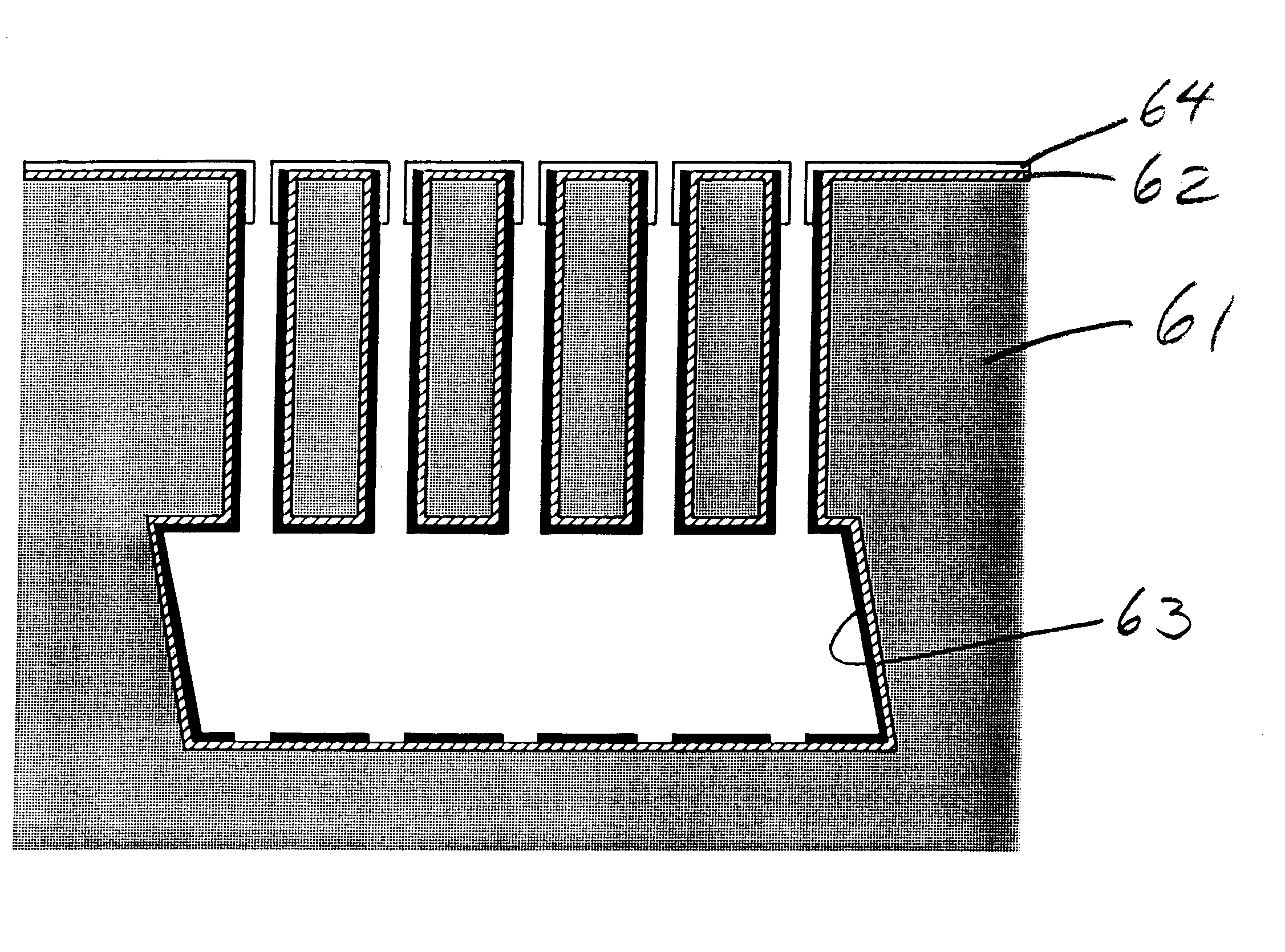
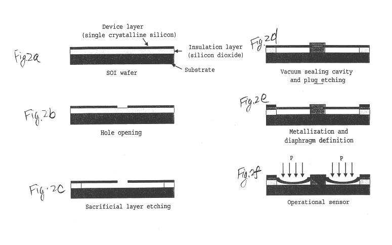
An aspect of the present invention provides a method for forming an electrode in a micromachined structure. The method includes providing a microstructure comprising silicon, the microstructure having at least one released surface opposite and spaced from an underlying surface of a substrate comprising silicon. An insulation layer is formed over surfaces of the microstructure, including over the released surface, a conductive layer is formed over surfaces of the insulation layer, and a metal layer is formed over at least a top surface of the conductive layer on at least a portion of the microstructure.

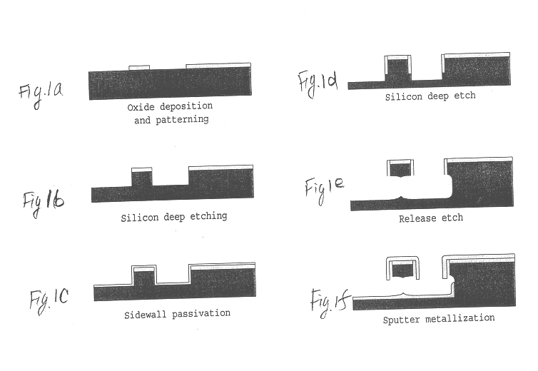
Another preferred isolation method forms an insulation layer on the exposed surfaces of a microstructure after the microstructure has been formed by micromachining and released from the surface of an underlying substrate. The isolation ...


PUM

PropertyMeasurementUnit
thicknessesaaaaaaaaaa

Abstract

An isolation method for a single crystalline silicon microstructure using a triple layer structure is disclosed. The method includes forming the triple layer composed of an insulation layer formed over an exposed surface of the silicon microstructure, a conductive layer formed over the entire insulation layer, and a metal layer formed over a top portion of the microstructure; and partially etching the conductive layer to form electrical isolation between parts of the microstructure. The method does not require a separate photolithography process for isolation, and can be effectively applied to microstructures having high aspect ratios and narrow trenches. Also disclosed are single crystalline silicon microstructures having a triple layer isolation structure formed using the disclosed method.

Description

The present application claims priority under 35 U.S.C. .sctn. 119 from Korean patent application No. 2000-37659, "Isolation Method for Single Crystalline Silicon Micro Structure Using Triple Layers," filed with the Korean Industrial Property Office on Jul. 3, 2000, which application is hereby incorporated by reference in its entirety.1. Field of the InventionThe present invention relates to micromachining and in particular to electrically isolating parts of silicon microstructures.2. Description of the Related ArtMicroelectromechanical systems include component structures with typical minimum dimensions on the order of a micron where the component structures can have elaborate shapes and perform a variety of complex functions. The component structures of microelectromechanical systems are formed on a semiconductor or glass substrate. Microelectromechanical systems include devices such as accelerometers that sense the acceleration of a moving object, gyroscopes that sense the angula...

Claims


Application Information

Patent Timeline
Patent Type & Authority Patents(United States)
IPC IPC(8): B81C1/00B81B3/00H01L21/70H01L21/764
CPCB81C1/0019H01L21/764B81C2201/0178B81C1/00
Inventor CHO, DONG-ILLEE, SANGWOOPARK, SANGJUN
Owner BARUN ELECTRONICS CO LTD
Why Eureka
Try Eureka