Method for forming a silicide of metal with a high melting point in a semiconductor device

Inactive Publication Date: 2003-05-27
RENESAS ELECTRONICS CORP
View PDF21 Cites 5 Cited by
  • Summary
  • Abstract
  • Description
  • Claims
  • Application Information

AI Technical Summary

Problems solved by technology

In the process described above, the following problems arise when the CoSi.sub.2 film is formed by employing the above conventional method.
Thus, an impurity-diffused region having a desired low resistance is difficult to achieve
Secondly, the initial withstand voltage of a gate electrode (or initial gate-oxide-film breakdown voltage) is low.

Method used


Image

  • Method for forming a silicide of metal with a high melting point in a semiconductor device
  • Method for forming a silicide of metal with a high melting point in a semiconductor device
  • Method for forming a silicide of metal with a high melting point in a semiconductor device

Examples


first embodiment

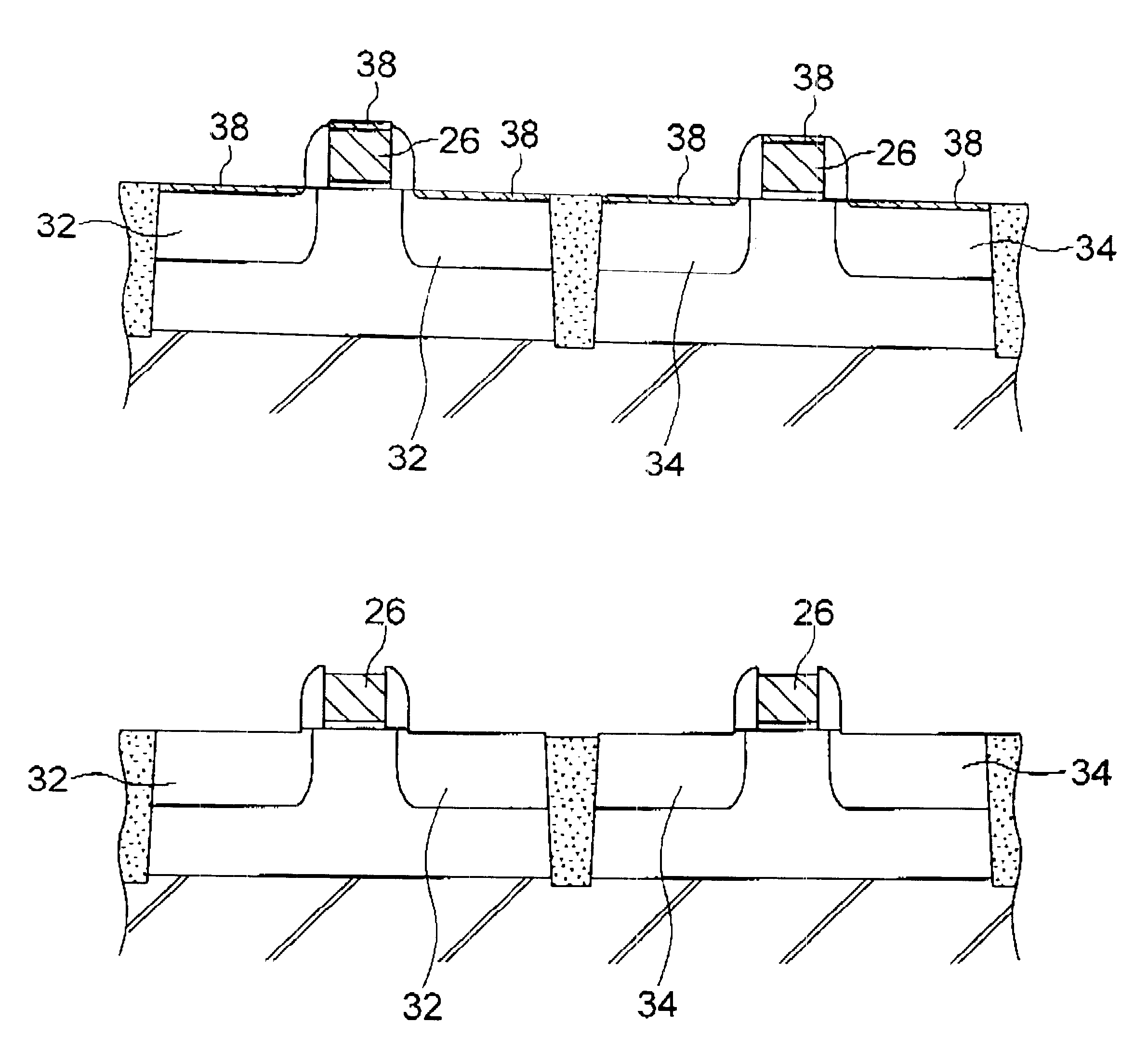
Referring to FIGS. 3A to 3E, a method for fabricating a CMOS device in accordance with a first embodiment of the present invention will be described. An element-isolation region 14 was formed on a silicon substrate 12 to form an NMOS forming region 16 and a PMOS forming region 18 as shown in FIG. 3A. Then, p-type impurities were implanted into the NMOS forming region 16 to form a P-well 20, and n-type impurities were implanted into the PMOS forming region 18 to form an N-well 22. Then, a gate oxide film 24 and a poly-crystalline-silicon layer were formed on the NMOS forming region 16 and the PMOS forming region 18, and the poly-crystalline-silicon layer was patterned to provide a gate electrode 26 having side walls 28 on its both side surfaces.

Then, a masking oxide film 30 was formed on the entire substrate surface by a known CVD method.

An arsenic ion was implanted as N-type impurities into the NMOS forming region 16 to form N-type impurity-implanted regions 32 at the both bottom si...

second embodiment

Referring to FIGS. 4A to 4D, a method for fabricating a CMOS device in accordance with a second embodiment of the present invention will be described. Description of an element shown in FIGS. 4A to 4D similar to the element shown in FIGS. 3A to 3E will be omitted by affixing the same numeral thereto.

At first, similarly to the first embodiment, a substrate having a masking oxide film 30 shown in FIG. 4A was obtained, and the masking oxide film 30 was removed. Thereby, higher-density areas 36 having a thickness of about 10 .ANG. and acting as a layer for inhibiting the reactions of cobalt and silicon were formed on a gate electrode 26, an N-type impurity-implanted regions 32, and a P-type impurity-implanted regions 34 as shown in FIG. 4B.

Then, in the present embodiment, a heat-treatment was conducted to the substrate under the following conditions for activating arsenic ions and boron ions 25 implanted into the N-type impurity-implanted regions 32 and the P-type impurity-implanted reg...


PUM


Abstract

A method for forming a silicide of a metal with high-melting-point in a semiconductor device includes the step of removing a higher-density impurity area which acts for prevention of forming the metal-silicide layer on the surface of the impurity-diffused region between the steps of implanting impurities to form an impurity-implanted region and annealing for reactions of cobalt and silicon of the diffused layer. The above-mentioned method of forming the metal-silicide layer on the surface of the impurity-diffused region proceeds smoothly to thereby prevent degradation of the initial gate withstand voltage and a higher sheet resistance.

Description

(a) Field of the InventionThe present invention relates to a method for forming a silicide of a metal with a high-melting-point in a semiconductor device, and more in particular, to the method for forming suicide of a metal with a high-melting-point on the surfaces of source / drain regions of a silicon substrate.(b) Description of the Related ArtSince a channel length is reduced with decrease of the line width of a gate electrode with the advance of the high integration of a semiconductor device, it is desired to suppress a short-channel effect in a MOSFET having shallower source / drain regions to thereby secure a desired source-drain withstand voltage.In a MOSFET including source / drain regions having the shallower junction, the gate delay time is liable to be extended due to the increase of the sheet resistance, whereby the operational frequency of a transistor is reduced to increase the length of a response time.In order to overcome the problem, the reduction of the resistance of th...

Claims


Application Information

Patent Timeline
IPC IPC(8): H01L21/285H01L21/28H01L21/02H01L21/336
CPCH01L21/28052H01L21/28512H01L29/665H01L21/28518H01L29/66545
Inventor HAMANAKA, NOBUAKIINOUE, KENMIKAGI, KAORU
Owner RENESAS ELECTRONICS CORP
Why Eureka
Try Eureka