

Stacked intelligent power module package
a power module and intelligent technology, applied in the field of semiconductor/solid-state device details, cooling/ventilation/heating modifications, printed circuit board receptacles, etc., can solve the problems of increasing the size of the leadframe and the power module package, increasing assembly manufacturing costs, and many problems
- Summary
- Abstract
- Description
- Claims
- Application Information
AI Technical Summary
Benefits of technology
Problems solved by technology
Method used
Image

Examples
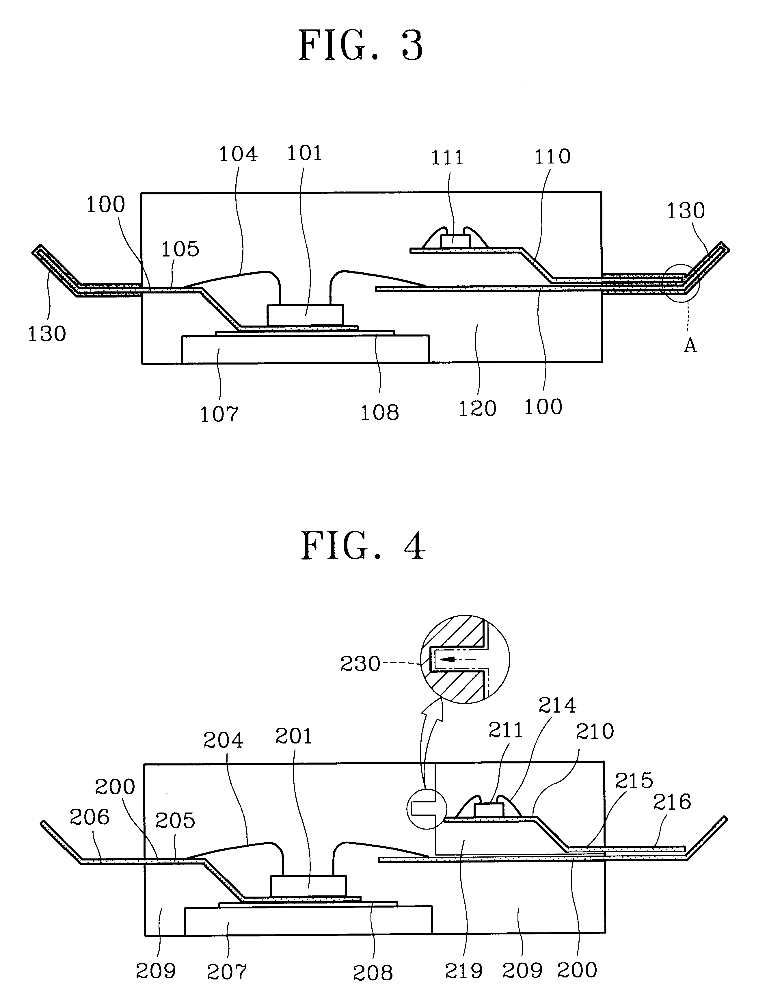
first embodiment
Intelligent Power Module Package With Stacked Leadframes
FIGS. 2 and 3 are cross sectional views illustrating an intelligent power module package and a method for manufacturing the same according to a first embodiment of the present invention.
Referring to FIG. 2, the structure and the elements of an intelligent power module package according to a first embodiment of the present invention, will be described.
In FIG. 2, an intelligent power module package according to a first embodiment of the present invention, includes a power unit, a heat sink 107, control unit and a sealing material 120. In the power unit, a chip 101 used in the power unit is bonded to a leadframe 100 of the power unit, which has a plurality of leads 105 and 106 formed at both of its sides and a chip pad formed in a down-set (DH of FIG. 2) with a depth (DH) range of 1-2 mm, and the chip 101 used in the power unit is bonded to each of a plurality of leads 105 with wires 104. Here, reference numerals 105 and 106 indic...
second embodiment
Intelligent Power Module Package With Stacked Semiconductor Packages
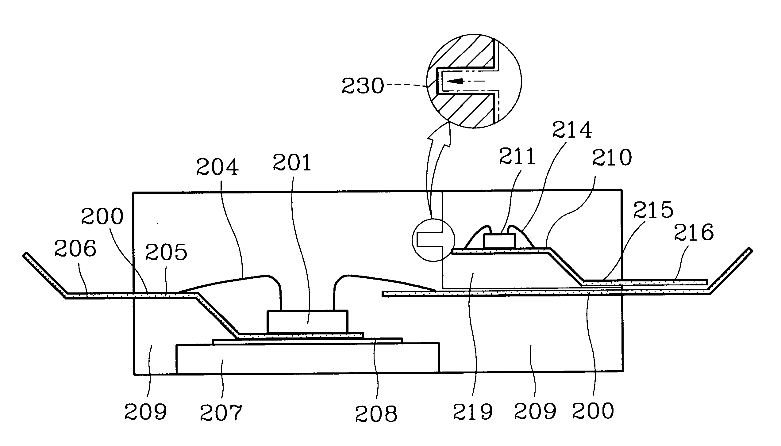
FIGS. 4 and 5 are cross sectional views illustrating an intelligent power module package and a method for manufacturing the same, according to a second embodiment of the present invention.
Here, a leadframe used in the second embodiment of the present invention, is the same as that of the first embodiment and parts of the second embodiment that are the same as those of the first embodiment will not be described.
Referring to FIG. 4, an intelligent power module package according to the second embodiment of the present invention includes two semiconductor packages of a power unit and a control unit, which are already processed by a molding process, a trimming / forming process, and an electrical property test. The two semiconductor packages are integrated into one semiconductor package by using a locking means 230 which is an inserting type.
The above semiconductor package of the power unit includes a leadframe 200 which h...
PUM
 Abstract
Description
Claims
Application Information