Pillar connections for semiconductor chips and method of manufacture

a technology of semiconductor chips and pillars, applied in the direction of welding/cutting media/materials, electrical equipment, solvents, etc., can solve the problems of constant reduction of the dimensions of the electronic devices on the silicon integrated circuit, device malfunction, and part occupied by air or another material not as effective in absorbing alpha particles, so as to reduce the chance of chip failure and stress in the connection

Inactive Publication Date: 2003-06-17
ADVANPAK SOLUTIONS PTE
View PDF16 Cites 571 Cited by
  • Summary
  • Abstract
  • Description
  • Claims
  • Application Information

AI Technical Summary

Benefits of technology

Using the elongated pillar of this invention, the separation between the solder in the pillar or any other solder used in the interconnect on the one hand and electronic devices on the semiconductor chip on the other hand can be made to exceed 55 microns or even 84 microns so that the electronic devices on the semiconductor chip will not be adversely effected by .alpha. particle emission from the solder when silicon dioxide or polyimide is used as the passivation layer. Where the length of the pillar ...

Problems solved by technology

As dimensions of the electronic devices on the silicon integrated circuits are continually reduced, .alpha. particle emissions by lead can cause significant problems.
As the dimensions of electronic devices in silicon integrated circuits become smaller, the distances between the lead-based solder and the devices are also reduced so that the .alpha. particle emission from the solder can cause such devices to malfunction.
Where silicon dioxide or another solid material is used as the passivation layer, only part of the medium separating the electronic devices from the solder is occupied by the material, with the remaining part occupied by air or another material not as effective in absorbing .alpha. particles.
Aside from the .alpha. particle emission problem described above, as the structural dimensions of electronic devices get smaller, the use of lead-based solder bumps is disadvantageous also because it may be difficult to achieve a fine pitch between adjacent interconnects without bridging which causes electrical shorting.
Th...

Method used


Image

  • Pillar connections for semiconductor chips and method of manufacture
  • Pillar connections for semiconductor chips and method of manufacture
  • Pillar connections for semiconductor chips and method of manufacture

Examples


Embodiment Construction

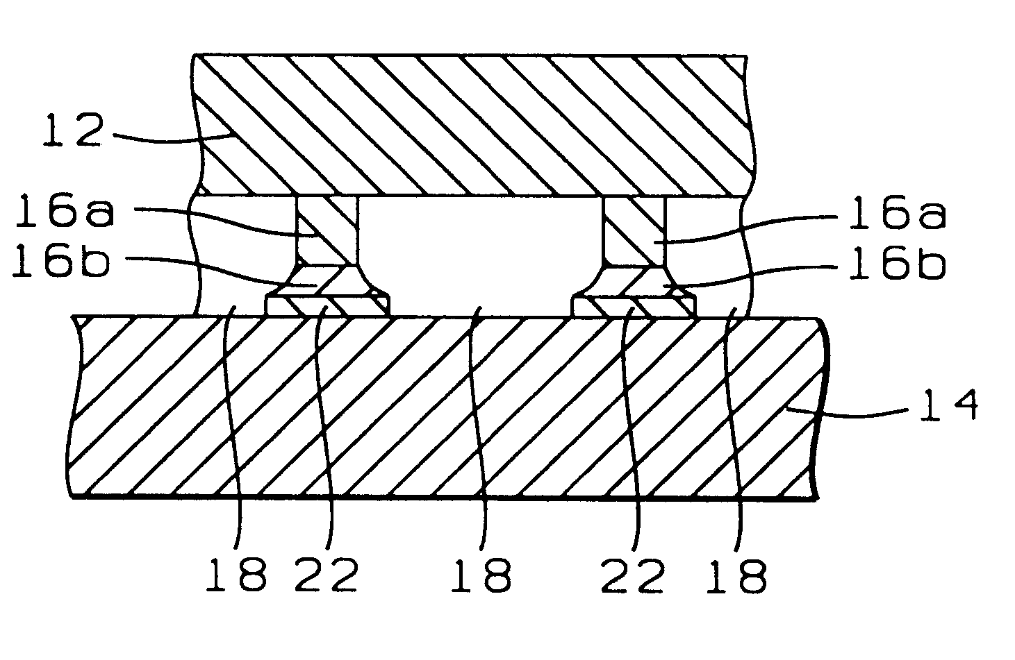
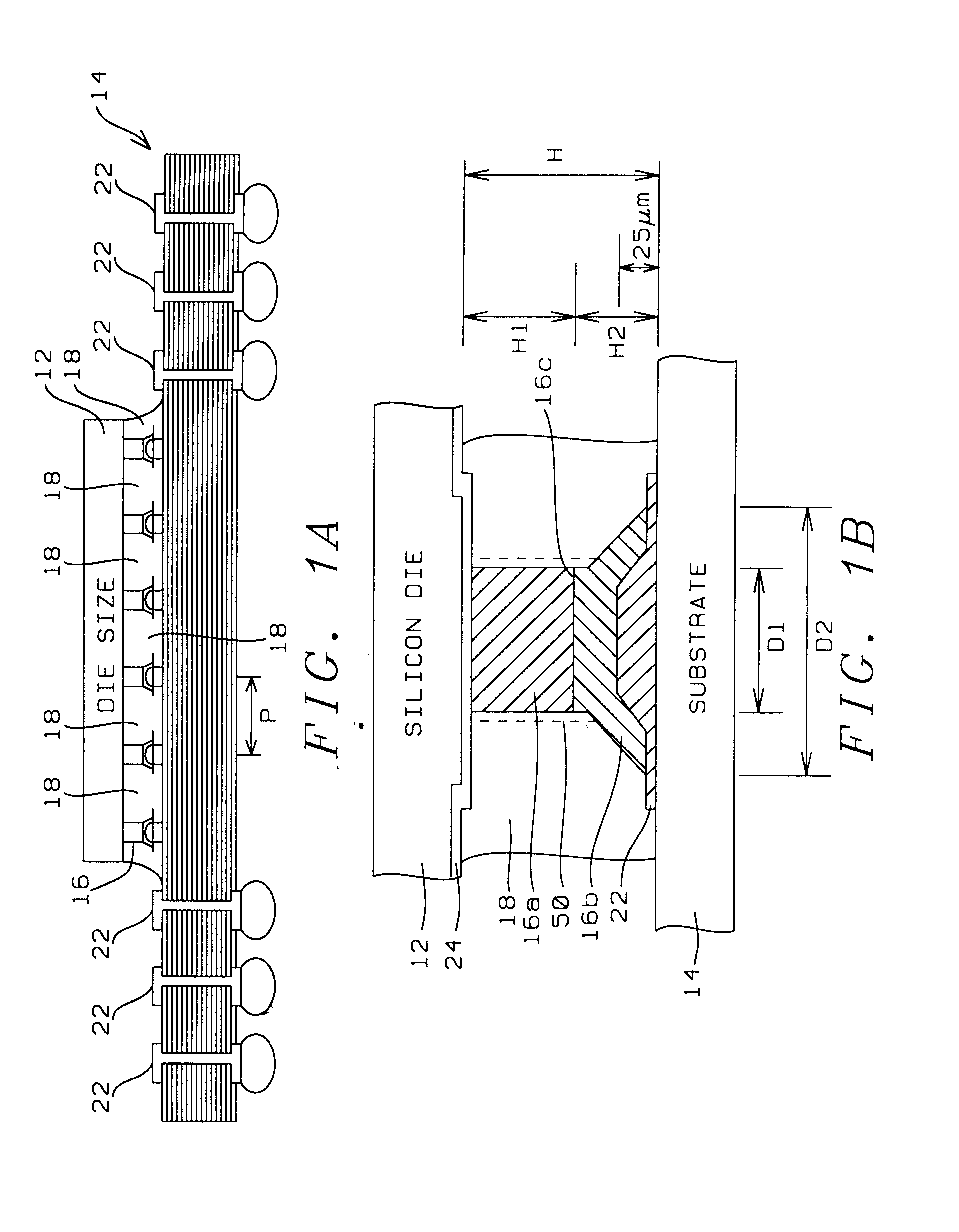
FIG. 1A is a cross-sectional view of a semiconductor die in the form of a flip chip 12 connected to a substrate 14 by means of elongated pillars 16 to illustrate an embodiment of the invention. As shown in FIG. 1A, the space between the die 12 and substrate 14 is filled with an underfill material 18 such as one known to those of skill in the art to provide support and stability to the die and interconnect structure formed by the elongated pillars 16.

FIG. 1B is an exploded view of a portion 1B of the system of FIG. 1A showing in more detail and elongated pillar connecting a portion of the silicon die to the substrate. As shown in FIG. 1B, pillar 16 comprises two parts: an upper elongated portion 16a comprising copper of height H1 and a second elongated portion of height H2 comprising a lead-based solder. The junction between the two portions 16a, 16b is at 16c. The bottom part of portion 16b is enlarged compared to its upper part and has a substantial conical shape where the bottom p...


PUM

PropertyMeasurementUnit
Lengthaaaaaaaaaa
Lengthaaaaaaaaaa
Lengthaaaaaaaaaa

Abstract

A flip chip interconnect system comprises and elongated pillar comprising two elongated portions, one portion including copper and another portion including solder. The portion including copper is in contact with the semiconductor chip and has a length preferably of more than 55 microns to reduce the effect of .alpha. particles from the solder from affecting electronic devices on the chip. The total length of the pillar is preferably in the range of 80 to 120 microns.

Description

BACKGROUND OF THE INVENTIONThis invention relates in general to interconnections for semiconductor devices and, in particular, to pillar-shaped connections from a semiconductor chip to a substrate and method for making the connections.Tin lead based solders is the preferred interconnect material of choice for flip chip bonding of silicon integrated circuits. As dimensions of the electronic devices on the silicon integrated circuits are continually reduced, .alpha. particle emissions by lead can cause significant problems. Lead has three stable isotopes which are formed as the end products of natural radioactive decay chains. These stable isotopes, however, usually contain a small amount of residual .alpha. particle radioactivity. As the dimensions of electronic devices in silicon integrated circuits become smaller, the distances between the lead-based solder and the devices are also reduced so that the .alpha. particle emission from the solder can cause such devices to malfunction.O...

Claims


Application Information

Patent Timeline
IPC IPC(8): H01L23/48H01L23/485
CPCH01L24/11H01L24/16H01L24/12H01L2924/10253H01L2224/1147H01L2224/11901H01L2224/1308H01L2224/13082H01L2224/13111H01L2224/13116H01L2224/13144H01L2224/13147H01L2224/13155H01L2224/16H01L2924/01013H01L2924/01015H01L2924/01022H01L2924/01029H01L2924/01039H01L2924/01046H01L2924/01047H01L2924/01074H01L2924/01078H01L2924/01079H01L2924/01082H01L2924/14H01L2924/15311H01L2924/3511H01L2224/73204H01L2224/32225H01L2224/16225H01L2924/014H01L2924/01033H01L2924/01024H01L2924/00013H01L2924/00014H01L2924/0105H01L2224/13099H01L2924/00H01L2224/29099H01L24/05H01L2224/05568H01L2224/05573H01L2224/05647H01L2224/05666H01L2224/05671H01L2224/13023
Inventor TUNG, FRANCISCA
Owner ADVANPAK SOLUTIONS PTE
Why Eureka
Try Eureka