PCB/complex electronic subsystem model

a technology of complex electronic subsystems and subsystems, applied in computing, instruments, electric digital data processing, etc., can solve the problems of time-consuming and repetitive existing processes, long and tedious processes, and opportunity for mistakes, and achieves easy adoption and use. , the effect of reducing the burden on software and hardware resources

Inactive Publication Date: 2003-07-01
AMPRO COMP
View PDF8 Cites 10 Cited by
  • Summary
  • Abstract
  • Description
  • Claims
  • Application Information

AI Technical Summary

Benefits of technology

An advantage of the present invention is that it does provide an improved system to incorporate a complex electronic system (CES) in to a printed circuit board (PCB) design, and it does this in highly efficient and easily adoptable manner.
Another advantage of the invention is that it permits the use of a library element for one or more CESs when designing PCBs. As such, as little as one library is needed, and that library need not contain data on the respective individual elements of the CES.
Another advantage of the invention is that its use of a library element approach to PCB design is less burdensome on the software and hardware resources used. The software design tools are not unduly burdened by the processing efforts of a macro approach or the excessive detail of a modular approach. The hardware is not unduly burdened by the need to store and manage large and multiple CIS or library databases, and additional processing is minimized. As is well known, an increase in element count produces an increase in processing which is quite non-linear. The other design as-if-with-separate-elements, macro, and modular approaches all require treatment of a CES essentially as all of its individual elements. The invention reduces it to a

Problems solved by technology

However, when a subassembly, such as a daughter card, has needed to be part of the design, the associated connectors have had to be placed individually, and the physical constraints manually designed and checked.
Not only can this be a long and tedious process, but it must be repeated for every new design using the same subassembly.
Clearly this existing process is time consuming and repetitive, and each time it is repeated there is an opportunity for mistakes to be made.
The problem, however, is the shear volume of data that must be managed, and the interrelationships between that data.
In view of the complexity of many PCB designs today, these files and templates may be quite large.
For instance, a component such as a micro processor may be developed in-house or may be so new that its manufacturer has not yet standardized and shipped a library component definition.
Modern PCB designs, however, tend to quickly become more complex than simply picking and placing collections of basic component elements.
PCB designers, however, tend to not be comfortable with macros and modules.
Both recorded and written macros, however, tend to suffer from two extremes, attempting to cover too little or too much at once.
A macro that is recorded is necessarily based on the state of the environment in which it is being recorded, and that environment may be quite complex.
Attempting to provide for all later eventualities can make the macro unduly large and slow, and inherently degrades into an automated form of macro writing, anyway.
In contrast, when a human writes a macro they tend to include too little because they are narrowly focused and have only a limited grasp of all of the variables and options available.
Both versions may work fine if the word processor is used in a "what you see is what you get" display mode, but one the other or both versions may produce undesired results

Method used


Image

  • PCB/complex electronic subsystem model
  • PCB/complex electronic subsystem model
  • PCB/complex electronic subsystem model

Examples


Embodiment Construction

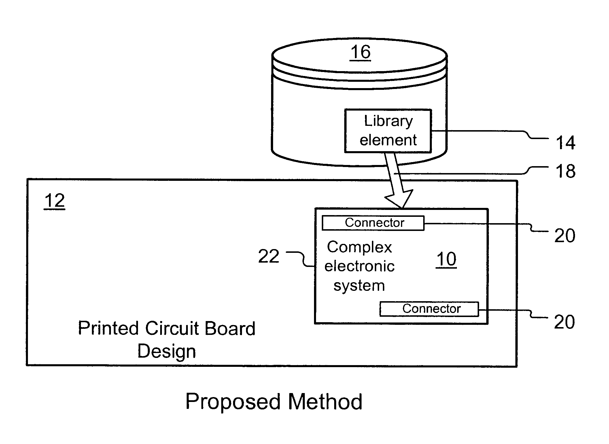
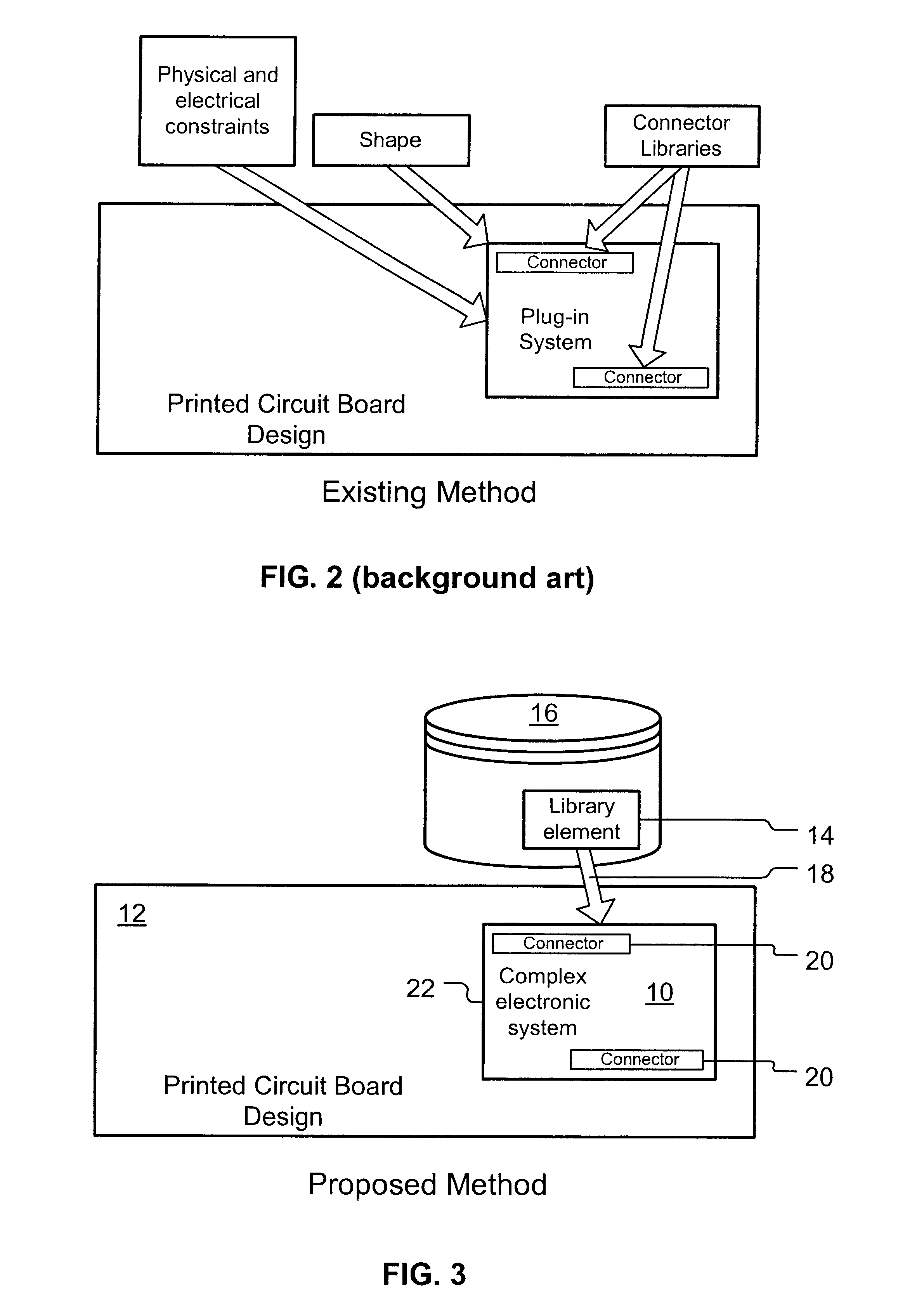
A preferred embodiment of the present invention is library element model of a complex electronic system (CES) for use in a printed circuit board (PCB). As illustrated in the various drawings herein, and particularly in the views of FIGS. 3-4, preferred embodiments of the invention are depicted by the general reference characters 14, 100.

FIG. 3 is a block diagram depicting in a stylized manner how the present invention permits a complex electronic system (CES 10) to be designed into a PCB 12, i.e., a work piece in the greater design scheme here. The CES 10 is represented as a library element 14, which may reside in and thus only require access to a single library 16 by a design tool 18. The CES 10, the library 16, and the design tool 18 may be essentially conventional. The CES 10 attaches to the PCB 12 by a plurality of connectors 20 (including a plurality of pads, not shown). The CES 10 also exhibits a footprint 22 with respect to the PCB 12, which is simply rectangle here.

For purpo...


PUM


Abstract

A process (100) and library element (14) product by that process for use with a design tool (18) to incorporate a complex electronic system (CES) (10) into a printed circuit board (PCB) (12) under development. The CES (10) is complex by virtue of having a plurality of connectors (20). The process (100) integrates physical data, and optionally also functional and other data, about the CES (10) into the library element (14). The library element (14) then may be stored and used from a conventional library (16) in the manner already widely used in the art for less complex elements.

Description

The present invention relates generally to electrical data processing, and more particularly to systems for circuit design and analysis of modular components. It is anticipated that primary application of the present invention will be in the design of application specific electrical data processing systems.Briefly, when laying out a printed circuit board (PCB) using a software tool, such as ALLEGRO, PADS, or OrCAD, each component needs to be modeled with a footprint and a definition of the component pins. However, when a subassembly, such as a daughter card, has needed to be part of the design, the associated connectors have had to be placed individually, and the physical constraints manually designed and checked. Not only can this be a long and tedious process, but it must be repeated for every new design using the same subassembly. Clearly this existing process is time consuming and repetitive, and each time it is repeated there is an opportunity for mistakes to be made.PCB design...

Claims


Application Information

Patent Timeline
IPC IPC(8): G06F17/50
CPCG06F17/5068G06F30/39
Inventor ROSENBAUM, ALANROSENFELD, PAUL I.
Owner AMPRO COMP
Why Eureka
Try Eureka