Highly latchup-immune CMOS I/O structures

a cmos i/o and latchup technology, applied in the field of structures and methods of fabricating integrated cmos circuits, can solve the problems of shrinking device dimensions, increasing the problem of self-destructive latchup effect of cmos circuits, and increasing so as to improve the latchup immunity, improve the effect of latchup immunity and reduce the spacing between nmos and pmos devices

Inactive Publication Date: 2003-09-02
TAIWAN SEMICON MFG CO LTD
View PDF5 Cites 21 Cited by
  • Summary
  • Abstract
  • Description
  • Claims
  • Application Information

AI Technical Summary

Benefits of technology

It is an object of the present invention to provide new CMOS I / O structures and methods which improve their latchup immunity.
Another object of the present invention is to decrease the spacing between the NMOS and PMOS devices to 5 micron while maintaining improved latchup immunity.
These objects have been achieved in a first preferred embodiment by inserting p+ and n+ diffusion guard-rings into the NMOS and PMOS source side of a semiconductor substrate, respectively. P+ diffusion guard-rings surround individual n-channel transistors and n+ diffusion guard-rings surround individual p-channel transistors. These guard-rings, connected to voltage supplies, reduce the shunt resistances of the parasitic SCRs, commonly associated with CMOS structures, from either the p-substrate to p+ guard-ring or the n-well to n+ guard-ring.
In a second preferred embodiment of the present invention a deep p+ implant is implanted into the p+ guard-ring or p-well pickup to decrease the shunt resistances of the parasitic SCRs. The n+ and p+ guard-rings, like the guard-rings of the first preferred embodiment, are connected to positive and negative voltage supplies, respectively. In either of the two preferred embodiments the shunt resistances are reduced to less than 3 Ohms, thereby preventing the forward biasing of the parasitic bipolar transistors of the SCR.

Problems solved by technology

The inherent and self-destructive latchup effect in CMOS circuits which has always been a major problem has become even more so a problem as device dimension continue to shrink.
When latchup occurs the circuit stops functioning and may even get destroyed because of the heat developed by the large currents.
Internal voltages across the anode and cathode of that SCR which exceed a breakover voltage cause the SCR to reach a low impedance state with the possibility of a resultant high current.
Another way to avoid latchup is to use EPI wafers to reduce the resistivity of the substrate resistor with a resultant higher cost.

Method used


Image

  • Highly latchup-immune CMOS I/O structures
  • Highly latchup-immune CMOS I/O structures
  • Highly latchup-immune CMOS I/O structures

Examples


Embodiment Construction

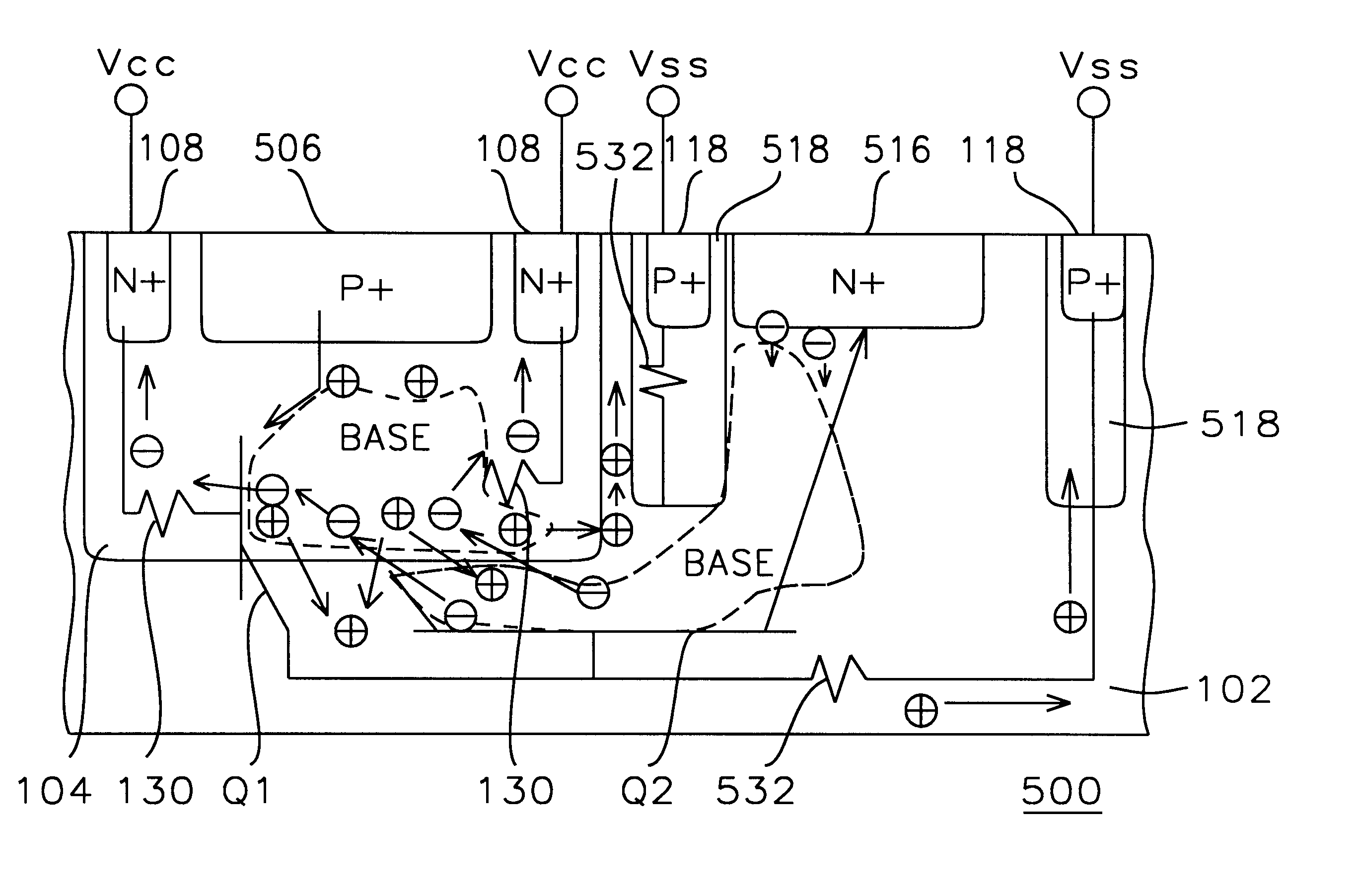
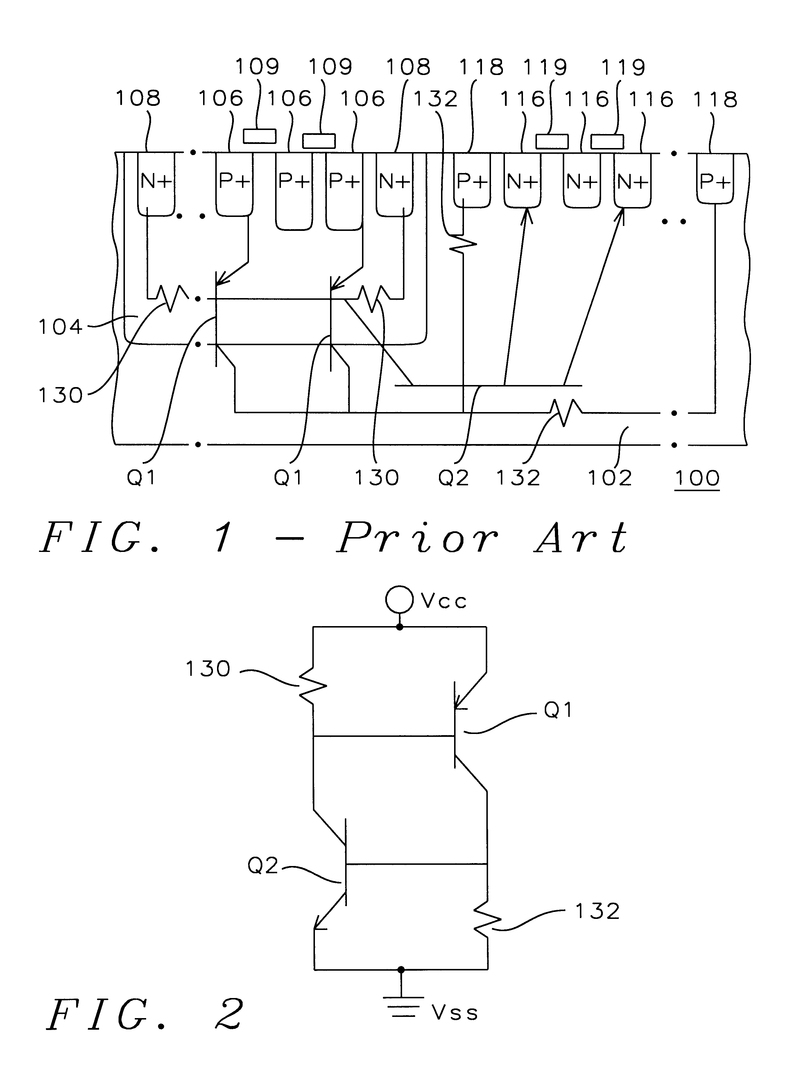
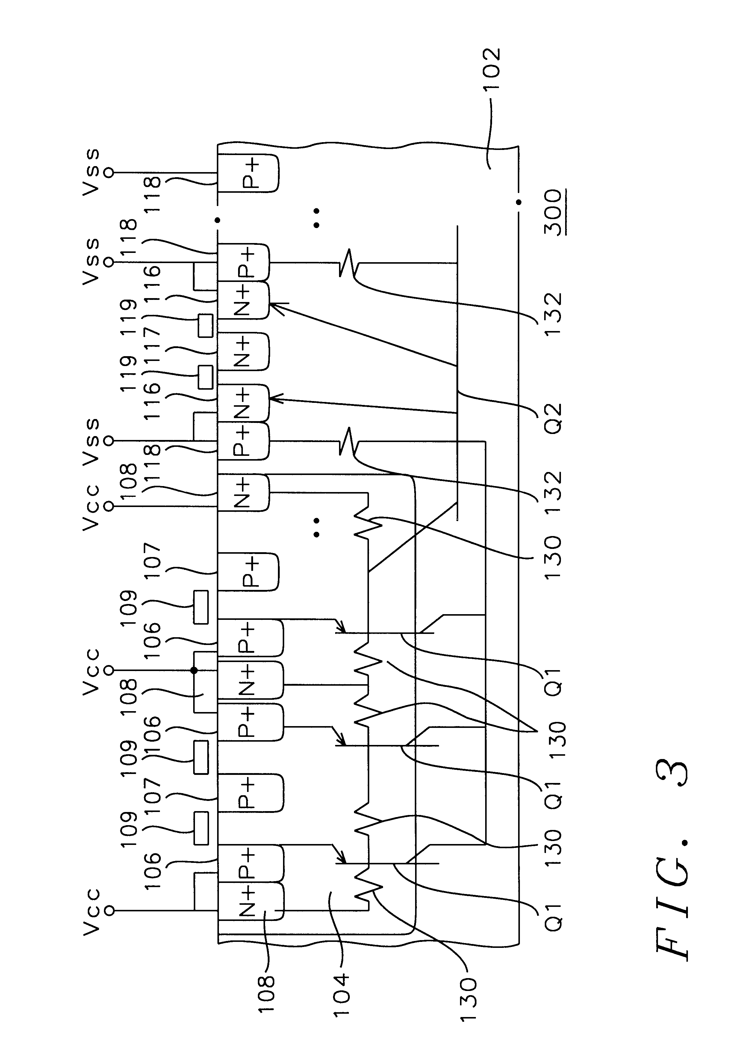
We now proceed with the description of a first preferred embodiment of the present invention by directing attention to FIG. 3. FIG. 3 shows a cross-sectional view of CMOS device layout 300. Embedded in a p-substrate 102 of a semiconductor wafer is an n-well 104 containing p+ source regions 106 and p+ drain regions 107. N+ guard-rings 108 surround individual regions 106 and 107, where regions 106 and 107 make up one or more p-channel transistors. N+ guard rings 108 and p+ source regions 106 are tied to a voltage supply V.sub.cc. Similarly, n+ source regions 116 and n+ drain regions 117 are formed in the p-substrate 102. P+ guard rings 118 surround individual regions 116 and 117, where regions 116 and 117 make up one or more n-channel transistors. P+ guard rings 118 and n+ source regions 116 are tied to voltage supply V.sub.ss which is more negative than V.sub.cc. Gates 109 are indicated straddling regions 106 and 107. Gates 119 similarly straddle regions 116 and 117. Q1 is a vertical...


PUM


Abstract

CMOS I/O structures are described which are latchup-immune by inserting p+ and n+ diffusion guard-rings into the NMOS and PMOS source side of a semiconductor substrate, respectively. P+ diffusion guard-rings surround individual n-channel transistors and n+ diffusion guard-rings surround individual p-channel transistors. These guard-rings, connected to voltage supplies, reduce the shunt resistances of the parasitic SCRs, commonly associated with CMOS structures, from either the p-substrate to p+ guard-ring or the n-well to n+ guard-ring. In a second preferred embodiment a deep p+ implant is implanted into the p+ guard-ring or p-well pickup to decrease the shunt resistances of the parasitic SCRs. The n+ and p+ guard-rings, like the guard-rings of the first preferred embodiment, are connected to positive and negative voltage supplies, respectively. In either of the two preferred embodiments the reduced shunt resistances prevent the forward biasing of the parasitic bipolar transistors of the SCR, thus insuring that the holding voltage is larger than the supply voltage.

Description

BACKGROUND OF THE INVENTION1. Field of the InventionThe invention relates to structures and methods of fabricating integrated CMOS circuits, and more particularly to making those CMOS circuits highly immune to latchup.2. Description of the Related ArtLatchup is a phenomenon of CMOS circuits well known to circuit designers and is described by S. Wolf in Silicon Processing for the VLSI Era, Volume 2, by Lattice Press, copyright 1990, 6.4 LATCHUP IN CMOS. The inherent and self-destructive latchup effect in CMOS circuits which has always been a major problem has become even more so a problem as device dimension continue to shrink. The latchup phenomenon creates a low resistance path between the positive and negative voltage supplies of a CMOS circuit and enables the flow of large currents through the affected circuit. When latchup occurs the circuit stops functioning and may even get destroyed because of the heat developed by the large currents.Latchup is caused by the presence of paras...

Claims


Application Information

Patent Timeline
Patent Type & Authority Patents(United States)
IPC IPC(8): H01L21/70H01L21/8238H01L27/092H01L27/085
CPCH01L21/823878H01L27/0921
Inventor LEE, JIAN-HSINGSHIH, JIAW-RENCHEN, SHUI-HUNGLIAO, PING-LUNG
Owner TAIWAN SEMICON MFG CO LTD
Why Eureka
Try Eureka