

Semiconductor laser device having thickened impurity-doped aluminum-free optical waveguide layers
a laser device and semiconductor technology, applied in the direction of lasers, lasers, semiconductor lasers, etc., can solve the problems of deterioration rate and semiconductor laser device deterioration, and achieve the effect of reducing the deterioration ra
- Summary
- Abstract
- Description
- Claims
- Application Information
AI Technical Summary
Benefits of technology
Problems solved by technology
Method used
Image

Examples
first embodiment
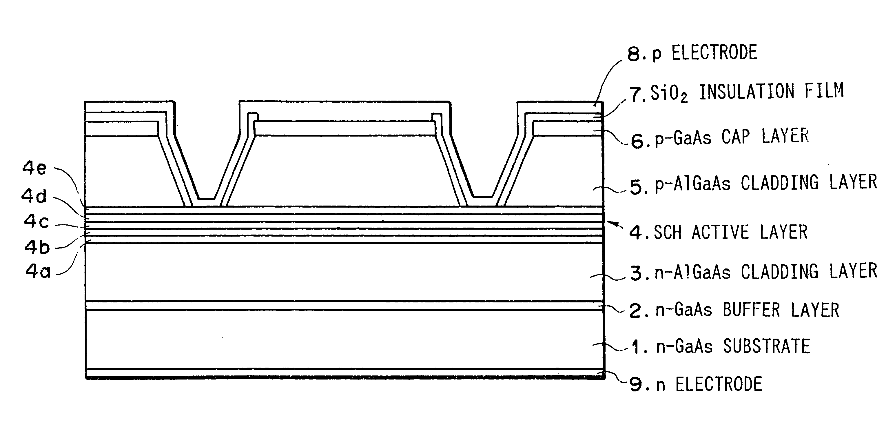
FIG. 1 is a cross-sectional view of a semiconductor laser device as the first embodiment of the present invention.
As illustrated in FIG. 1, an n-type GaAs buffer layer 2 being doped with 5.times.10.sup.17 cm.sup.-3 Si and having a thickness of 0.5 .mu.m, an n-type Al.sub.0.63 Ga.sub.0.37 As cladding layer 3 being doped with 5.times.10.sup.17 cm.sup.-3 Si and having a thickness of 1 .mu.m, an undoped SCH (separate confinement heterostructure) active layer 4, a p-type Al.sub.0.63 Ga.sub.0.37 As cladding layer 5 being doped with 7.times.10.sup.17 cm.sup.-3 Zn and having a thickness of 1 .mu.m, a p-type GaAs cap layer 6 being doped with 2.times.10.sup.19 cm.sup.-3 Zn and having a thickness of 0.3 .mu.m, and a SiO.sub.2 insulation film 7 are formed on an n-type GaAs substrate 1 which is doped with 2.times.10.sup.18 cm.sup.-3 Si.
The undoped SCH active layer 4 is formed of an n-type In.sub.0.48 Ga.sub.0.52 P optical waveguide layer 4a being doped with 5.times.10.sup.17 cm.sup.-3 Si and hav...
second embodiment
FIG. 6 is a cross-sectional view of a semiconductor laser device as the second embodiment of the present invention.
As illustrated in FIG. 6, an n-type GaAs buffer layer 42 being doped with 1.times.10.sup.18 cm.sup.-3 Si and having a thickness of 0.5 .mu.m, an n-type Al.sub.0.55 Ga.sub.0.45 As cladding layer 43 being doped with 1.times.10.sup.18 cm.sup.-3 Si and having a thickness of 1 .mu.m, an SCH active layer 44, an n-type Al.sub.0.65 Ga.sub.0.35 As current confinement layer 45 being doped with 1.times.10.sup.18 cm.sup.-3 Si and having a thickness of 0.8 .mu.m, an n-type GaAs protection layer 46 being doped with 1.times.10.sup.18 cm.sup.-3 Si and having a thickness of 0.01 .mu.m, a p-type Al.sub.0.55 Ga.sub.0.45 As cladding layer 47 being doped with 1.times.10.sup.18 cm.sup.-3 Zn and having a thickness of 1 .mu.m, and a p-type GaAs cap layer 48 being doped with 2.times.10.sup.19 cm.sup.-3 Zn and having a thickness of 0.3 .mu.m are formed on an n-type GaAs substrate 41 which is dop...
third embodiment
FIG. 7 is a cross-sectional view of a semiconductor laser device as the third embodiment of the present invention.
As illustrated in FIG. 7, an n-type GaAs buffer layer 62 being doped with 1.times.10.sup.18 cm.sup.-3 Si and having a thickness of 0.5 .mu.m, an n-type Al.sub.0.6 Ga.sub.0.4 As cladding layer 63 being doped with 1.times.10.sup.18 cm.sup.-3 Si and having a thickness of 1 .mu.m, an undoped SCH active layer 64, an n-type Al.sub.0.65 Ga.sub.0.35 As current confinement layer 66 being doped with 1.times.10.sup.18 cm.sup.-3 Si and having a thickness of 0.8 .mu.m, an n-type GaAs protection layer 67 being doped with 1.times.10.sup.18 cm.sup.-3 Si and having a thickness of 0.1 .mu.m, a p-type Al.sub.0.6 Ga.sub.0.4 As first cladding layer 65 being doped with 1.times.10.sup.18 cm.sup.-3 Zn and having a thickness of 0.9 .mu.m, a p-type Al.sub.0.6 Ga.sub.0.4 As second cladding layer 68 being doped with 1.times.10.sup.18 cm.sup.-3 Zn and having a thickness of 1 .mu.m, and a p-type GaAs...
PUM
 Abstract
Description
Claims
Application Information