Electronic fuse structure and method of manufacturing

a fuse device and electronic technology, applied in the direction of semiconductor devices, electrical equipment, semiconductor/solid-state device details, etc., can solve the problems of complex manufacturing of each of these fuse devices in the prior art, and many processing steps

Inactive Publication Date: 2003-10-14
GOOGLE LLC
View PDF21 Cites 70 Cited by
  • Summary
  • Abstract
  • Description
  • Claims
  • Application Information

AI Technical Summary

Benefits of technology

It is a further object of the present invention to provide a novel high-performance signal line structure in integrated circuits and a method for manufacture thereof that is designed and tailored to minimize inter level signal capacitive loading.
The present invention solves the problem of removing an inter level dielectric selective to an overpassing conductor, and leaving an air gap between the conductor and the structure below, in a minimum of process steps. Thus, the present invention provides a solution to two known problems: 1) the minimization of inter level signal wiring capacitance with a material that has a low dielectric constant, e.g., an air gap; and, 2) locally minimizing the thermal conduction path below a conductor to the silicon substrate. The general method used to remove the underlying dielectric of an overpassing metal conducting line, e.g., aluminum or copper line, is to add one blockout mask to the process used to etch the region under the conductor.

Problems solved by technology

The manufacture of each of these fuse devices in the prior art is generally complicated requiring many processing steps.

Method used


Image

  • Electronic fuse structure and method of manufacturing
  • Electronic fuse structure and method of manufacturing
  • Electronic fuse structure and method of manufacturing

Examples


first embodiment

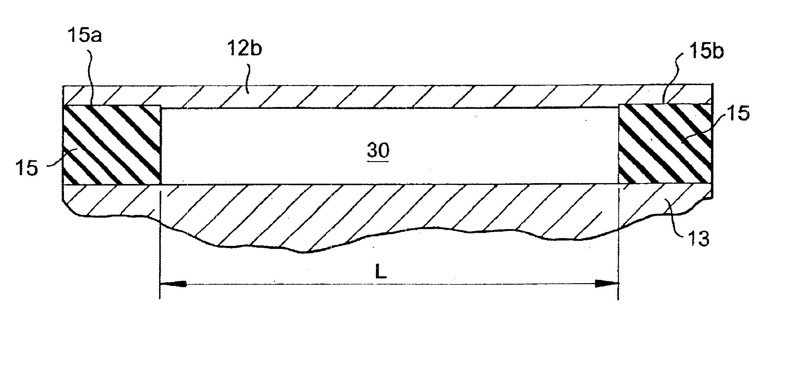
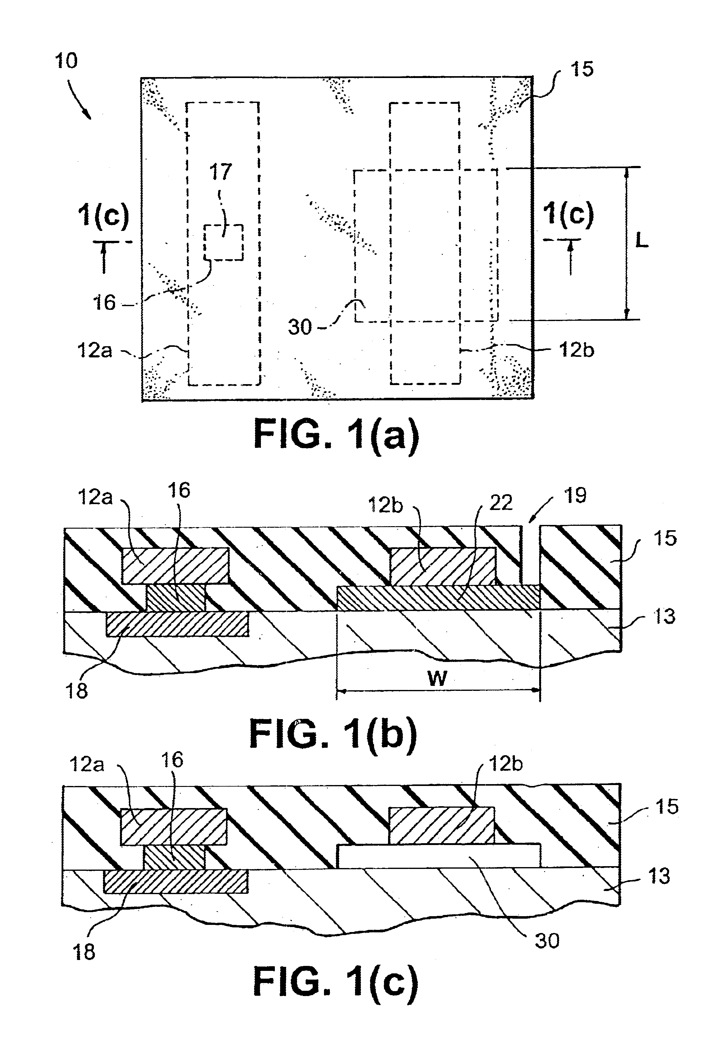
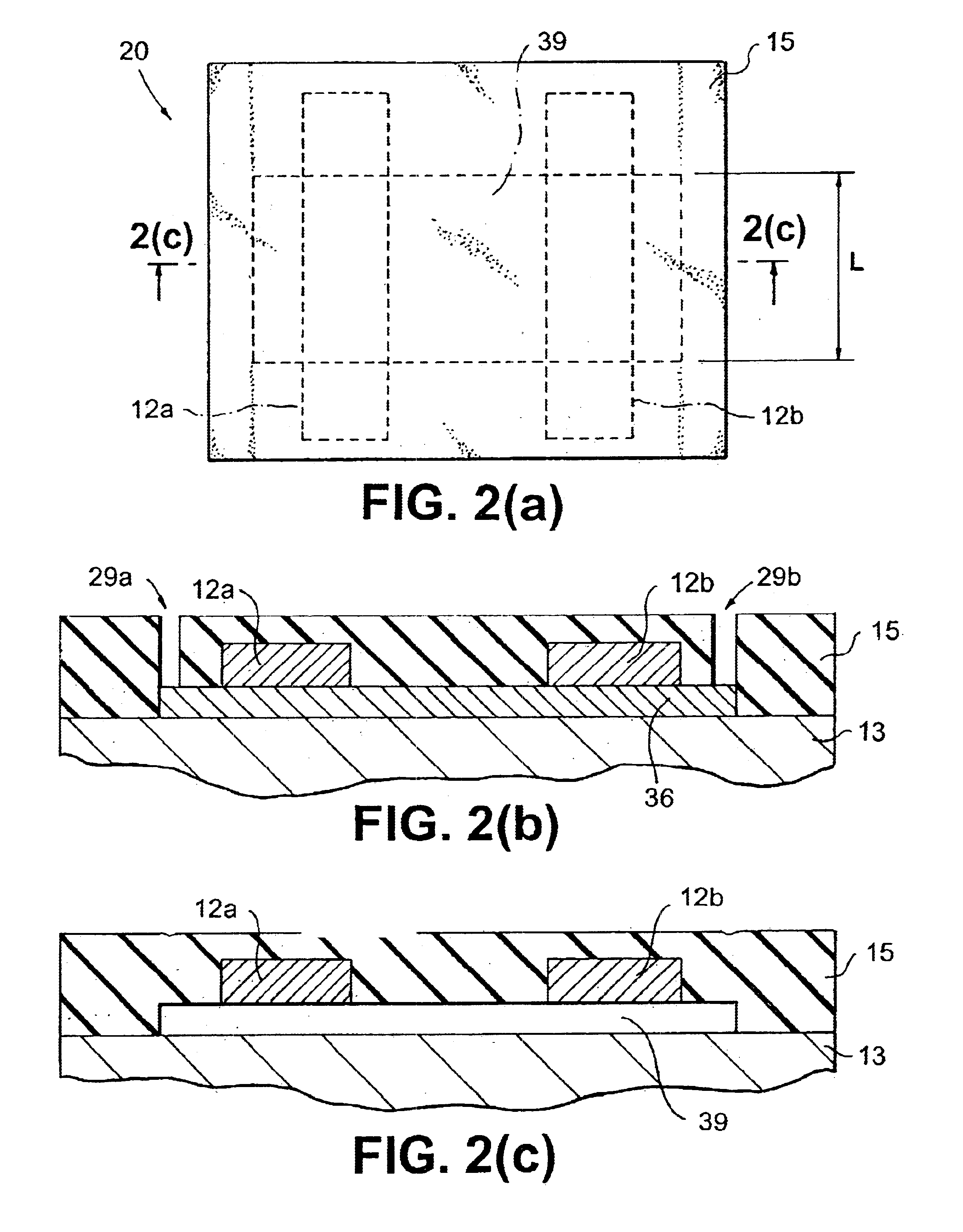
Further according to the principles described herein with respect the invention, a process is implemented to provide an air gap below two or more interlevel conductors. FIG. 2(a) illustrates a top view of a resultant fuse structure 20 including two conductors 12a, 12b each of which is a gap conductor having a gap 40 formed thereunder. Insulative material 15 is shown surrounding each of the conductors and the gap. As shown in FIGS. 2(a) and 2(b), an enlarged stud 36 of a typical composition material such as Ti / TiN liner filled with Tungsten, such as used in 64-1 Gb DRAM processing, is formed atop the insulative substrate 15, with each of the conductors 12a,b formed thereon in a subsequent processing step. An insulative layer 15 is then formed atop the conductive and underfill (stud) layer in a subsequent step. The enlarged stud 36 is to be used as a sacrificial gap-conductor underfill, with the underfill region 36 preferably designed to have a width "W" overextending the width of eac...

second embodiment

Finally, the via 49 is filled with insulator and the structure is planarized to result in a gap-conducting structure having gaps on all sides of the conductor 12b as shown in FIG. 3(c). Further according to the principles described herein with respect to the invention, a process is implemented to provide an air gap above and below two or more interlevel conductors. FIG. 4(a) illustrates a top view of a resultant fuse structure 60 including two conductors 12a, 12b each of which is a gap conductor having a gap region 55 formed thereabout. Preferably, both the underfill and overfill layers are designed to occupy a width "W" overextending the width of each conductor 12a,b, as shown in FIG. 1(a), and has a pre-defined length "L" which is less than the length of the corresponding conductor.

As shown in FIG. 4(b), an underfill layer stud 65 of width W and length L is first provided, as described above with respect to FIGS. 2(a) and 1(b), and, in a metallization step (Al or Cu), the respecti...


PUM


Abstract

A gap conductor structure for an integrated electronic circuit that may function as an electronic fuse device or as a low capacitance inter level signal line is integrated as part of the semi-conductor chip wiring. The gap conducting structure includes one or more air gap regions of predefined volume that fully or partially exposes a length of interlevel conductor layer in an IC. Alternately, the air gap region may wholly located within the dielectric region below a corresponding conductor and separated by insulator. When functioning as a fuse, the gap region acts to reduce thermal conductivity away from the exposed portion of the conductor enabling generation of higher heat currents in the conducting line with lower applied voltages sufficient to melt a part of the conducting line. The presence of gaps, and hence, the fuses, are scalable and may be tailored to the capacity of currents they must carry with the characteristics of the fuses defined by a circuit designer. Furthermore, conducting structures completely or partially exposed in the air gap may function as low capacitance minimum delay transmission lines.< / PTEXT>

Description

1. Field of the InventionThe present invention relates generally to electronic fuse structures provided in integrated circuits, and particularly, a system and method for fabricating scalable electronic fuse structures employed for fixing configuration of IC circuit components and enhancing IC circuit performance.2. Discussion of the Prior ArtCurrently, metal fuses may be fabricated in integrated circuits for a variety of reasons, including protection from ESD during manufacture and handling during burn-in or prior to packaging, removing or disconnecting defective components from a circuit, or, for generating initial values of stored data, e.g., in an IC ROM.U.S. Pat. No. 4,272,753 discusses a method for fabricating a discrete metallic fuse device using fusable material which is necked to a narrow region. The fusable material is separated from an insulative layer by an air gap which provides lower thermal conductivity environment.U.S. Pat. No. 4,089,734 discusses a metallic fuse devi...

Claims


Application Information

Patent Timeline
Patent Type & Authority Patents(United States)
IPC IPC(8): H01L23/52H01L23/525
CPCH01L23/5256H01L2924/0002H01L2924/00
Inventor BERTIN, CLAUDE L.HEDBERG, ERIK L.LEVY, MAX G.SULLIVAN, TIMOTHY D.TONTI, WILLIAM R.
Owner GOOGLE LLC
Why Eureka
Try Eureka