Composite member comprising bonded different members and method for making the composite member
a composite member and different member technology, applied in the direction of metal-working equipment, non-electric welding apparatus, metal-layered products, etc., can solve the problems of increasing the production cost of these composite members, generating thermal stress, and unable to achieve desired bonding strength or air tightness
- Summary
- Abstract
- Description
- Claims
- Application Information
AI Technical Summary
Problems solved by technology
Method used
Image

Examples
example 2
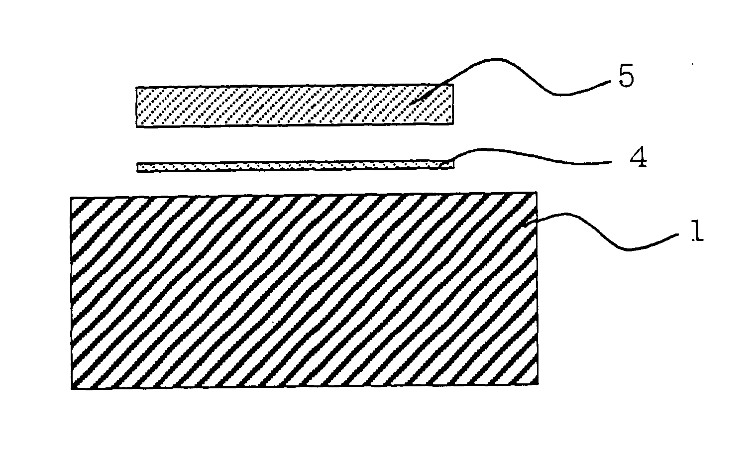
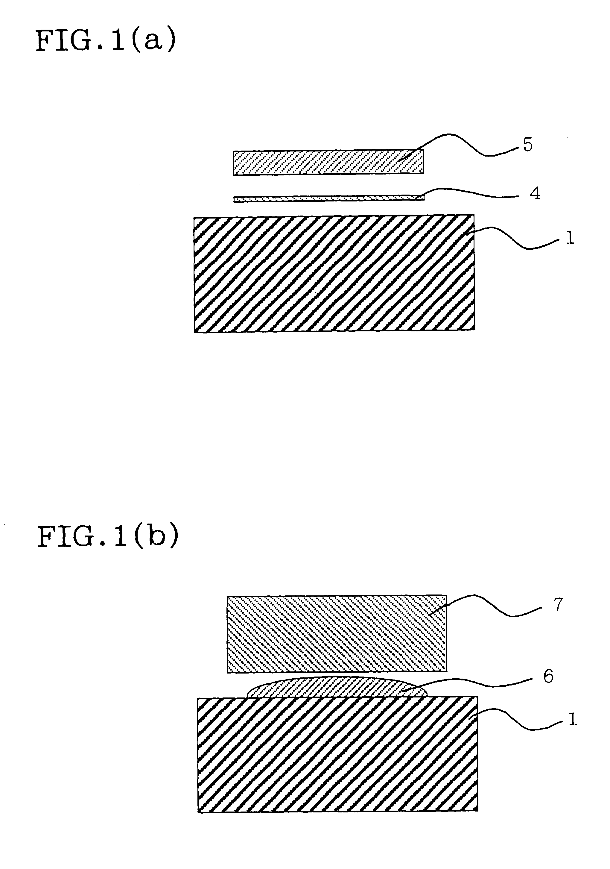
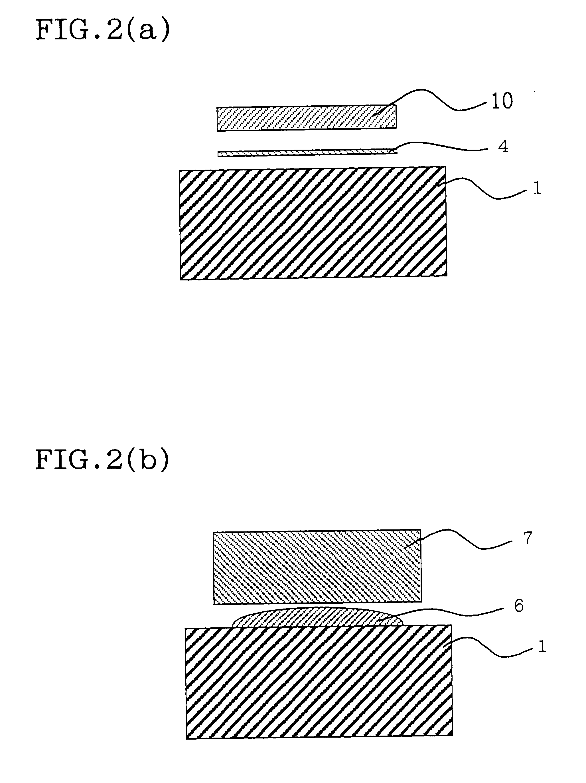
In an AlN base (30.times.30 mm.times.20 mm thick) were embedded an Mo mesh (a wire mesh prepared by knitting Mo wires of 0.12 mm .O slashed. in diameter at a density of 50 wires per 1 inch) and an electrical conductor (a molded body obtained by molding Mo powders of 1-100 .mu.m in particle diameter: 3 mm .O slashed. in diameter) which was electrically connected to the Mo mesh, and the portion of the AlN base in which the electrical conductor was embedded was bored, thereby exposing the electrical conductor. On the surface including this electrical conductor and the circumference thereof were disposed a Ti foil (5 .mu.m in thickness) and a solder material (0.3 mm in thickness) having the composition as shown in Table 1, followed by subjecting to heat treatment at 1100.degree. C. for 10 minutes in a vacuum atmosphere to perform soldering onto the AlN base. An Ni terminal (5 mm .O slashed. in diameter) was disposed on the solder layer, followed by subjecting to solid phase bonding by a...
example 3
In an AlN base (200 mm .O slashed. in diameter.times.20 mm in thickness) were embedded an Mo mesh (a wire mesh prepared by knitting Mo wires of 0.12 mm .O slashed. in diameter at a density of 50 wires per 1 inch) and a plurality of electrical conductors (molded bodies obtained by molding Mo powders of 1-100 .mu.m in particle diameter: 3 mm .O slashed. in diameter) which were electrically connected to the Mo mesh, and the portion of the AlN base in which the electrical conductors were embedded was bored, thereby exposing the electrical conductors. On the surface including these electrical conductors and the circumference thereof were disposed a Ti foil (5 .mu.m in thickness) and a solder material (0.3 mm in thickness) having the composition as shown in Table 2, followed by subjecting to a heat treatment at 1100.degree. C. for 10 minutes in a vacuum atmosphere to perform soldering onto the AlN base. An Ni terminal (5 mm .O slashed. in diameter) was disposed on the bonding layer, follo...
PUM
| Property | Measurement | Unit |
|---|---|---|
| temperature endurance | aaaaa | aaaaa |
| thickness | aaaaa | aaaaa |
| melting point | aaaaa | aaaaa |
Abstract
Description
Claims
Application Information