Strained fin FETs structure and method

a technology of fin fets and strained fins, which is applied in the direction of transistors, semiconductor devices, electrical equipment, etc., can solve the problems of reducing performance and/or reliability, several difficulties arise in the design and fabrication of double gated cmos transistors, and it is difficult to reliably fabricate one with reliable performance and minimum feature siz

Inactive Publication Date: 2003-10-21
MICROSOFT TECH LICENSING LLC
View PDF3 Cites 239 Cited by
  • Summary
  • Abstract
  • Description
  • Claims
  • Application Information

AI Technical Summary

Benefits of technology

Physical strain on the channel material in FETs can improve carrier mobility. Strain induced on planar p-type metal oxide semiconductor field effect transistor (MOSFET) devices has been shown to increase hole mobility in excess of 30%. This invention provides these advantages to thin semiconductor bodies that are vertically arranged on a substrate; and, as such, the invention combines greater channel control with greater carrier mobility.

Problems solved by technology

Unfortunately, increased device density in CMOS FETs often results in degradation of performance and / or reliability.
Unfortunately, several difficulties arise in the design and fabrication of double gated CMOS transistors.
First, the relative dimensions of a double gated transistor are such that it is difficult to reliably fabricate one that has reliable performance and minimum feature size.
In particular, current fabrication techniques have generally resulted in a double gated transistor that has either too high a threshold voltage or too low a threshold voltage.
The strain-producing layer has a sufficient concentration of germanium to produce strain within the central portion to enhance carrier mobility without producing sufficient dislocations to reduce overall performance of the transistor.

Method used


Image

  • Strained fin FETs structure and method
  • Strained fin FETs structure and method
  • Strained fin FETs structure and method

Examples


second embodiment

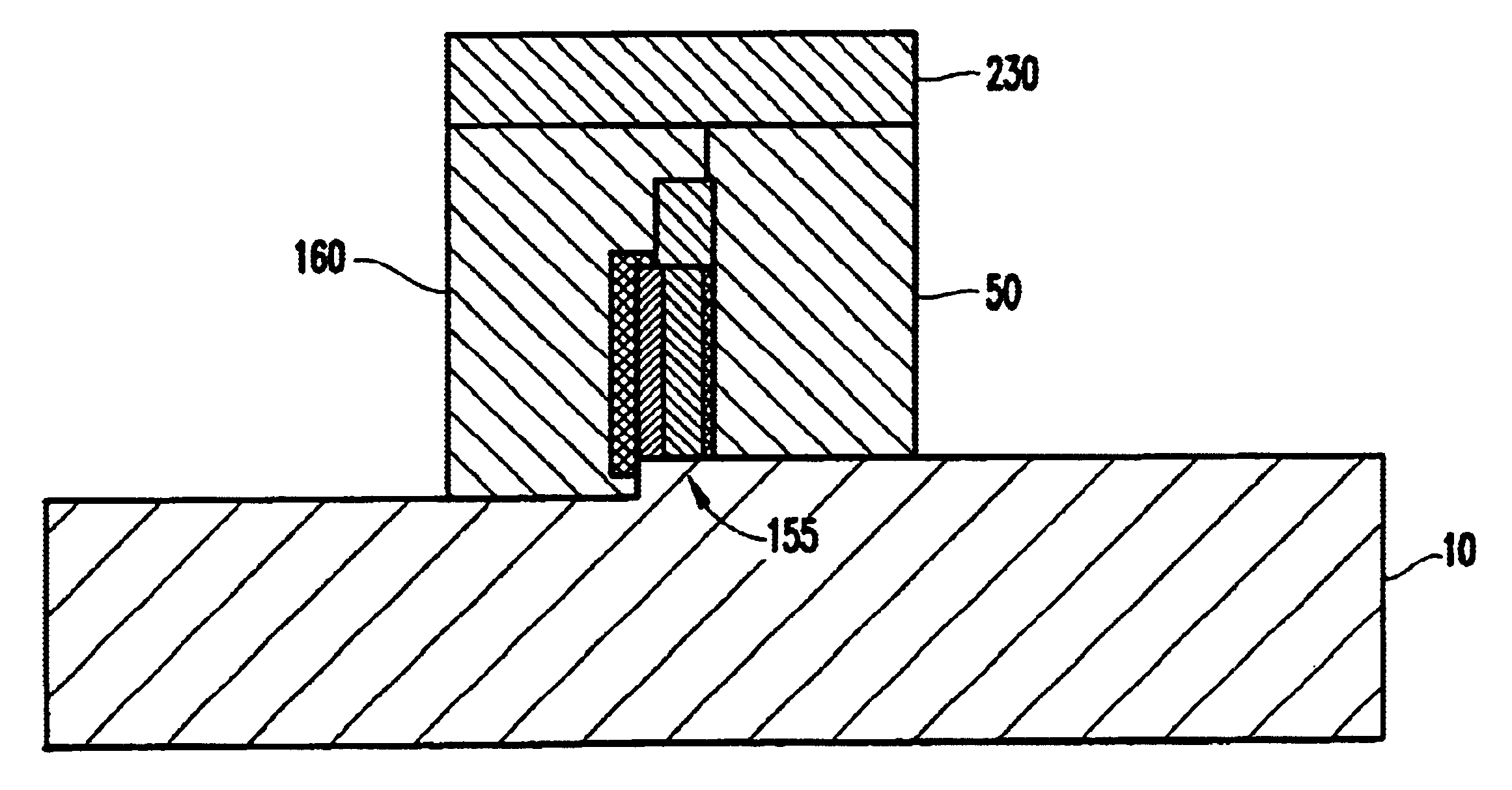
While the invention is described above with respect to an asymmetric strained Fin FET, it is equally applicable to a symmetric strained Fin FET. More specifically, as shown in FIGS. 29-31, the processing necessary to create a strained symmetric strained Fin FET in accordance with the invention starts with a SOI structure having a SiGe layer 300 above and insulator 10 (this is shown in FIG. 29). The SiGe layer 300 is selectively patterned, as shown in FIG. 30. Then, a silicon layer 315 is grown on the SiGe layer 300 to create a strained structure. A thermal oxide 320 is then grown on the silicon layer 315. Next, the gate conductors (e.g., polysilicon) 310 are deposited, planarized, and patterned to form the gates surrounding the body structure 155. In one embodiment, the gate conductors 310 have the same doping concentration and material makeup. However, in a different embodiment, the gate electrodes 310 can be made asymmetric with, for example, an ion implant, to result in an asymme...

first embodiment

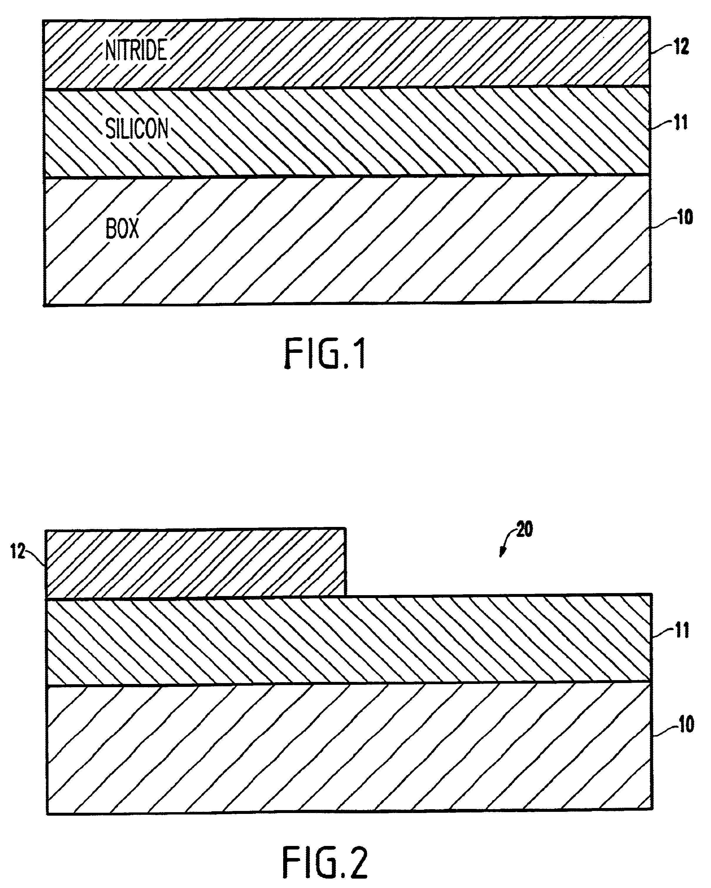
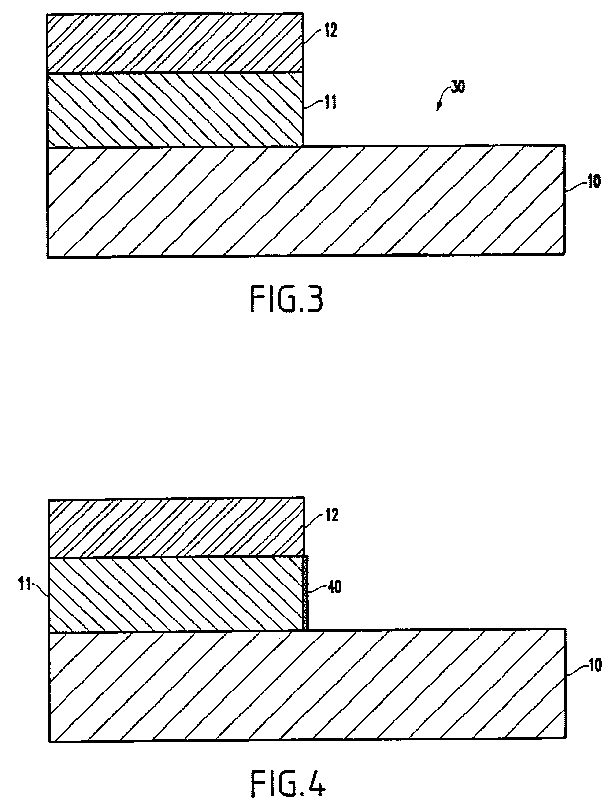
The formation of a Fin FET according to the invention is shown in FIGS. 1-28. Processing begins as shown FIG. 1 where a silicon over an insulator (SOI) structure includes an insulator 10 such as a buried oxide layer with an overlying silicon layer 11. A placeholder layer 12 (such as a nitride, etc.) is deposited over the silicon layer 11. This structure is then patterned using well-known conventional patterning processes, as shown in FIG. 2, to remove a portion 20 of the placeholder layer 12. A subsequent etching step removes any corresponding portion 30 of the silicon layer 11 not protected by the placeholder 12, as shown in FIG. 3.

In FIG. 4, an oxidation process grows a gate oxide layer 40 on the silicon 11. Next, polysilicon 50 is deposited over the structure, as shown FIG. 5. The polysilicon 50 is of one dopant type (e.g., N+ doped polysilicon, etc.). In FIG. 6, the structure is planarized using, for example, a chemical mechanical polishing (CMP) process to form planar layer 60....


PUM


Abstract

A method and structure for a transistor that includes an insulator and a silicon structure on the insulator. The silicon structure includes a central portion and Fins extending from ends of the central portion. A first gate is positioned on a first side of the central portion of the silicon structure. A strain-producing layer could be between the first gate and the first side of the central portion of the silicon structure and a second gate is on a second side of the central portion of the silicon structure.

Description

1. Field of the InventionThe present invention generally relates to the field of semiconductor manufacturing and, more specifically, to a method for forming double-gated field effect transistors.2. Description of the Related ArtThe need to remain cost and performance competitive in the production of semiconductor devices has caused continually increasing device density in integrated circuits. To facilitate the increase in device density, new technologies are constantly needed to allow the feature size of these semiconductor devices to be reduced.The push for ever-increasing device densities is particularly strong in complementary metal oxide semiconductor (CMOS) technologies, such as the in the design and fabrication of field effect transistors (FETs). FETs are used in almost all types of integrated circuit design (i.e., microprocessors, memory, etc.). Unfortunately, increased device density in CMOS FETs often results in degradation of performance and / or reliability.One type of FET ...

Claims


Application Information

Patent Timeline
Patent Type & Authority Patents(United States)
IPC IPC(8): H01L29/10H01L21/02H01L29/786H01L21/336H01L29/66H01L29/02
CPCH01L29/1054H01L29/66795H01L29/78687H01L29/78603H01L29/785H01L21/18H01L21/28H01L21/22
Inventor CLARK, WILLIAM F.FRIED, DAVID M.LANZEROTTI, LOUIS D.NOWAK, EDWARD J.
Owner MICROSOFT TECH LICENSING LLC
Why Eureka
Try Eureka