Sputtering device

a technology of sputtering device and sputtering rate, which is applied in the direction of electrodes, diaphragms, ion implantation coatings, etc., can solve the problems of reducing the roughness of the film surface, increasing the probability of gas atom-electron collision, and reducing the sputtering ra

Inactive Publication Date: 2003-11-04
DATA STORAGE INST
View PDF11 Cites 28 Cited by
  • Summary
  • Abstract
  • Description
  • Claims
  • Application Information

AI Technical Summary

Benefits of technology

The combination of planar-magnetron-sputtering-cathodes and facing-targets-sputtering-cathodes in a single device has the advantage that a wide range of deposition requirements can be met. Each planar-magnetron-sputtering-cathode and each facing-targets-sputtering-cathode are preferably mounted for rotation about a common axis between a working position in which the respective cathode is used to deposit a layer on a substrate, and a non-working position in which the respective cathode is not used to deposit a layer on said substrate. Preferably, electrical connections to the planar-magnetron-sputtering-cathode and the pair of facing-targets-sputtering-cathode are shielded to atmospherically isolate them from the single vacuum chamber.
According to a preferred embodiment, the planar-magnetron-sputtering-cathode and the facing-targets-sputtering-cathode can be positioned for sputtering deposition onto a substrate in an arbitrary sequence, and the device is adapted such that a substrate can be spun during deposition of a layer thereon. The device is preferably further adapted such that the distance between the surface of a substrate to be subject to deposition and the planar-magnetron-sputtering-cathode and / or the facing-targets-sputtering-cathode can be varied. The device is also preferably adapted such that the distance between the two facing targets of the facing-targets-sputtering-cathode can be varied. In a preferred embodiment, the two facing targets are mounted for movement along a common rail such that the distance between them can be varied.

Problems solved by technology

This results in an increase in the gas atom-electron collision probability and leads to a much higher sputtering rate than that obtained without the use of magnetic confinement.
This results in a decreased roughness of film surface and only a relatively small rise in substrate temperature.

Method used


Image

  • Sputtering device
  • Sputtering device
  • Sputtering device

Examples


first embodiment

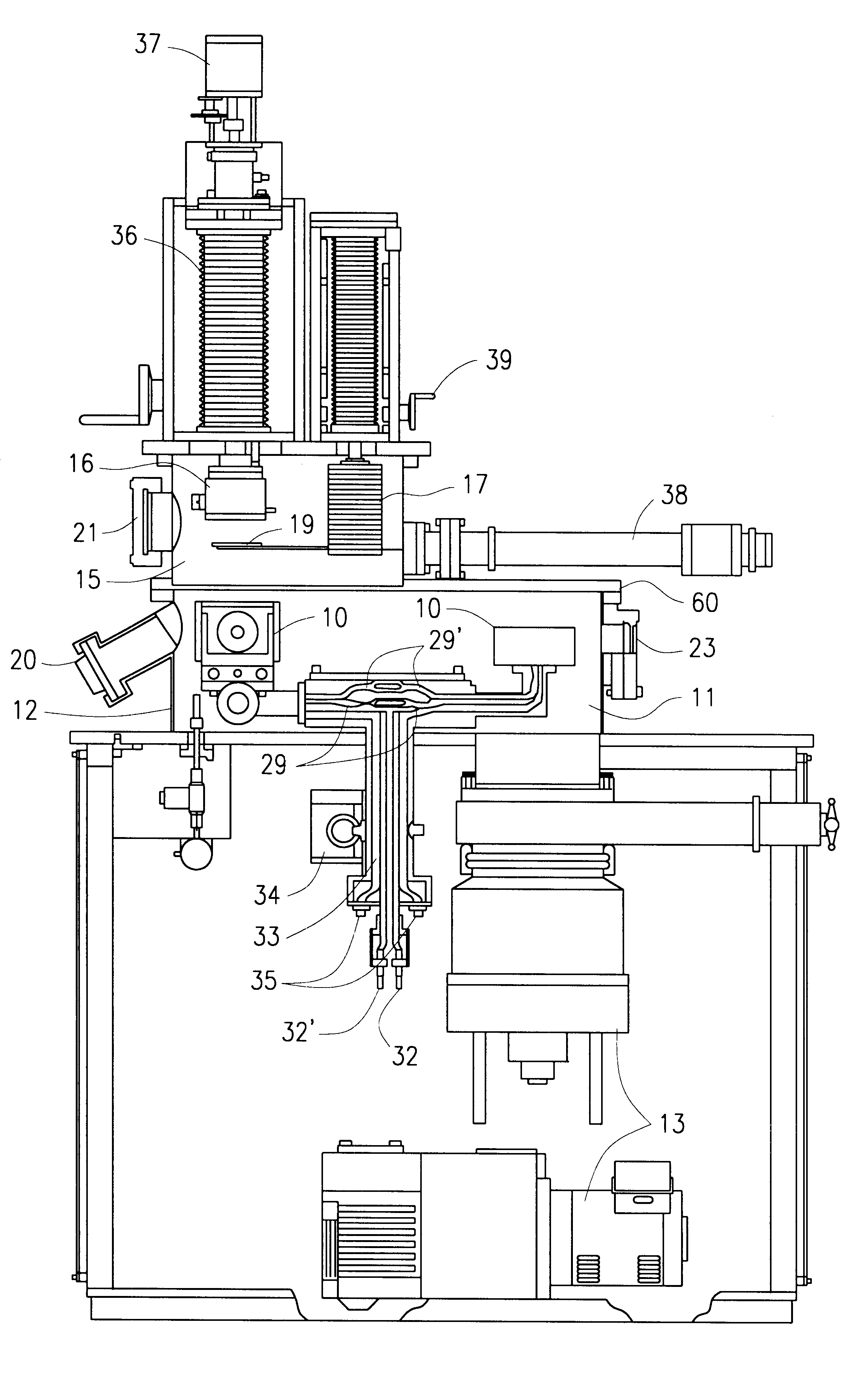
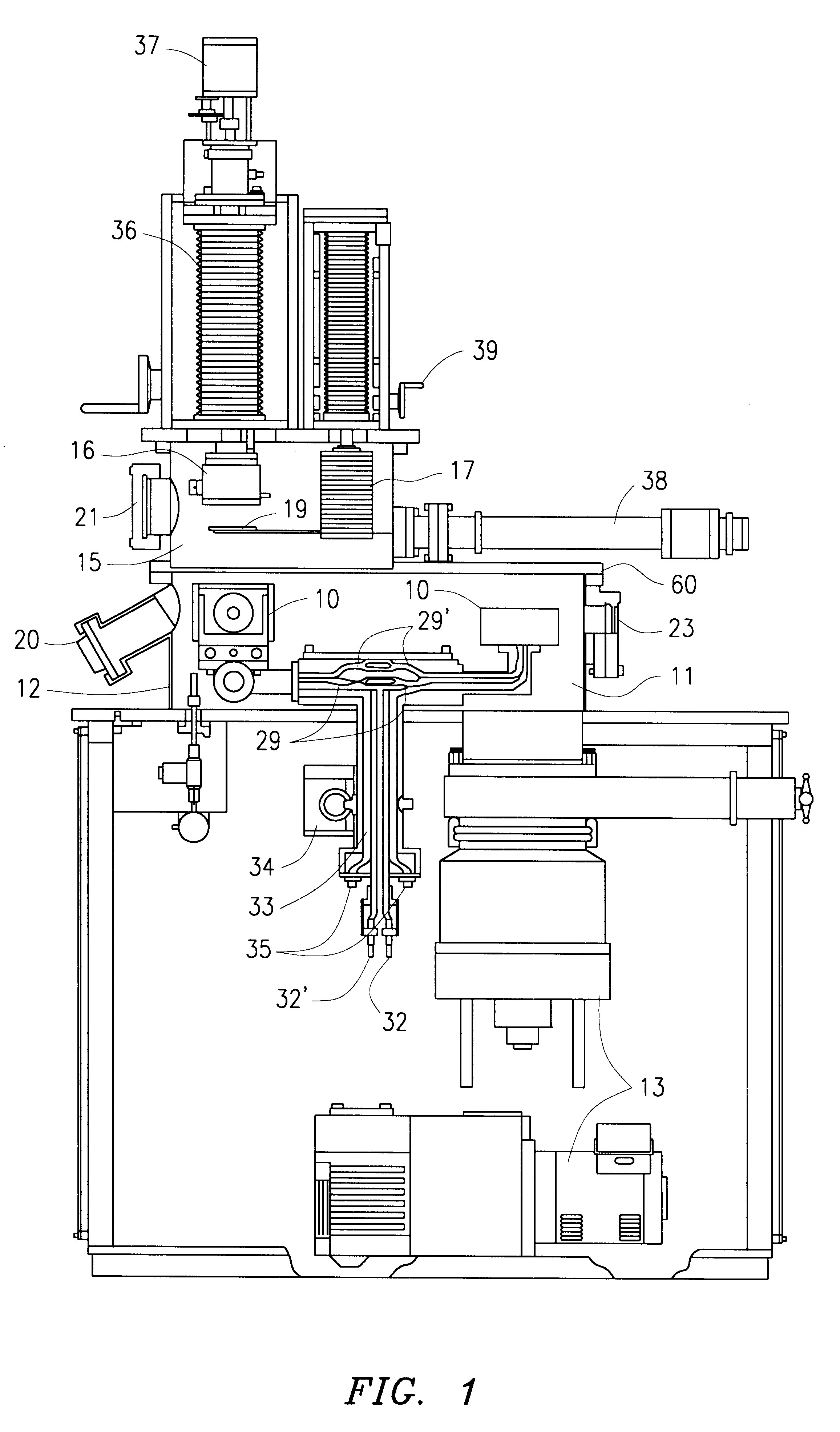
A cross-sectional view of a device in accordance with the present invention is illustrated in FIG. 1. A cathode assembly 10 is positioned in a sputtering chamber 11 enclosed by a chamber housing 12 which can be evacuated by a suitable vacuum pumping means 13 and can be back-filled by a gas-supplying component 14 with a suitable gas such as Argon. On the left side of the upper chamber 15 is a substrate holder 16. On the right side of the upper chamber is a cassette 17 accommodating several substrates.

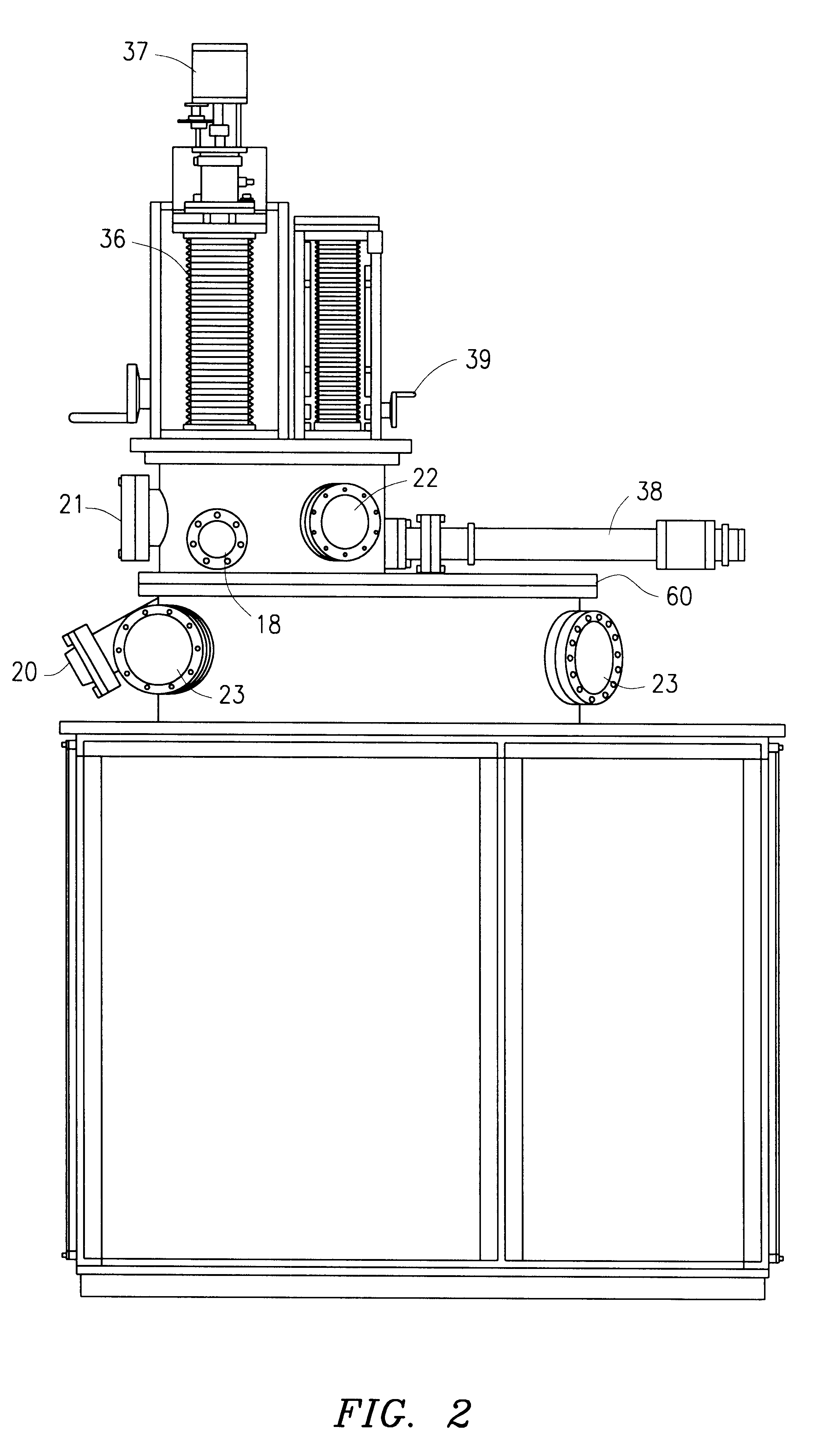
A front view of the device is illustrated in FIG. 2. In the wall of the upper vacuum chamber, a first set of two quartz flanges 18 (only one is shown) are mounted to oppose each other. The center axes of the flanges 18 are oriented to be at an angle with respect to the surface of the substrate 19 (see FIG. 1) during sputtering, and can be used for in-situ optical analysis such as Ellipsometry analysis and optical multi-channel analysis of the film. The first set of two quartz flanges 18 ...

second embodiment

In the device, all cathodes are fixed when sputtering is carried out, as illustrated in FIG. 5 and FIG. 6. Below the main chamber 41 are provided several small chambers or stations 42 (only 4 are shown). The symmetric centers of all the stations 42 are positioned on a circle's circumference 9 having a suitable diameter, as shown in FIG. 6. In each station is provided a planar-magnetron-sputtering-cathode 43 or a pair of facing-targets-sputtering-cathode 44. The distance between two facing targets in each pair of facing-targets-sputtering-cathode can be varied within a suitable range via the feedthrough. The main chamber and each station have their own vacuum pumping means and gas-supplying component (not shown). Each station has the same dimensions, thereby allowing for the exchange of stations with one another. In addition, certain positions in the station housing are provided with black flanges 45 having a size equivalent to that of the feedthrough of the two types of cathodes. Th...

third embodiment

the cathode assembly has an open in-line configuration as illustrated in FIG. 7a. It consists of several planar-magnetron-sputtering stations 50 (only two shown), several facing-targets-sputtering stations 51 (only two shown), a sample-loading station 52, a pre-treating station 53, and a sample-unloading station 54. Each sputtering station may contain several pairs of facing targets 57 (only one pair shown) or several planar magnetron targets 56 (only one shown). All cathodes are fixed during deposition of film. In the pre-treating station 53, heating of the substrate or RF etching of the substrate is carried out. The substrates are transferred on a sample pallet from station to station by a driving means( not shown). Between two neighbouring stations is provided a passage for transferring substrates. Each station is separated from one another by a vacuum valve 55. Each station has the same connection size, so that the arraying sequence of the stations can be exchanged. For example,...


PUM

PropertyMeasurementUnit
distanceaaaaaaaaaa
distancesaaaaaaaaaa
movementaaaaaaaaaa

Abstract

The present invention is directed to a sputtering device for depositing multi-layer films on a substrate, the sputtering device comprising at least one planar-magnetron-sputtering-cathode and at least one facing-targets-sputtering-cathode housed in a single vacuum chamber, and adapted such that each planar-magnetron-sputtering-cathode and facing-targets-sputtering-cathode can be selectively positioned for sputtering deposition onto a substrate.

Description

1. Field of the InventionThe present invention relates generally to a sputtering device, and more particularly to an integrated device for forming multi-layer thin film structures on a substrate, and to a method for depositing at least one layer of film on a substrate using such a device.2. Description of Related ArtCoating of a substrate by sputtering is a well established art. Deposition by sputtering is generally performed as follows: Atoms of an inert gas such as Argon (Ar) are ionized into positive ions by a glow discharge. These positive ions are accelerated toward a cathode or target by an electric field and then impinged upon the target. As a result of the ionic bombardment, neutral atoms and ions are transferred from the target surface into a vacuum chamber due to the exchange of momentum there between. The liberated or sputtered atoms and ions are consequently deposited on a pre-selected substrate disposed in the vacuum chamber.In planar-magnetron-sputtering, the cathode i...

Claims


Application Information

Patent Timeline
Patent Type & Authority Patents(United States)
IPC IPC(8): C23C14/35C23C14/56
CPCC23C14/568C23C14/352
Inventor SHI, JIAN ZHONGWANG, JIAN PING
Owner DATA STORAGE INST
Why Eureka
Try Eureka