Electro-optical device

a technology of optical devices and optical components, applied in static indicating devices, non-linear optics, instruments, etc., can solve problems such as signal delay and increase in manufacturing steps

Inactive Publication Date: 2004-02-10
SEMICON ENERGY LAB CO LTD
View PDF5 Cites 66 Cited by
  • Summary
  • Abstract
  • Description
  • Claims
  • Application Information

AI Technical Summary

Problems solved by technology

In the conventional liquid crystal display device in which a metallic film is used as the light shielding mask of the color filter, there arose a problem in that a parasitic capacitor is generated with the other wiring to easily cause a delay in signal.
Besides, in the case an organic film containing a black pigment is used as the light shielding mask of the color filter, there arose a problem in the number of manufacturing steps increases.

Method used


Image

  • Electro-optical device
  • Electro-optical device
  • Electro-optical device

Examples


embodiment 1

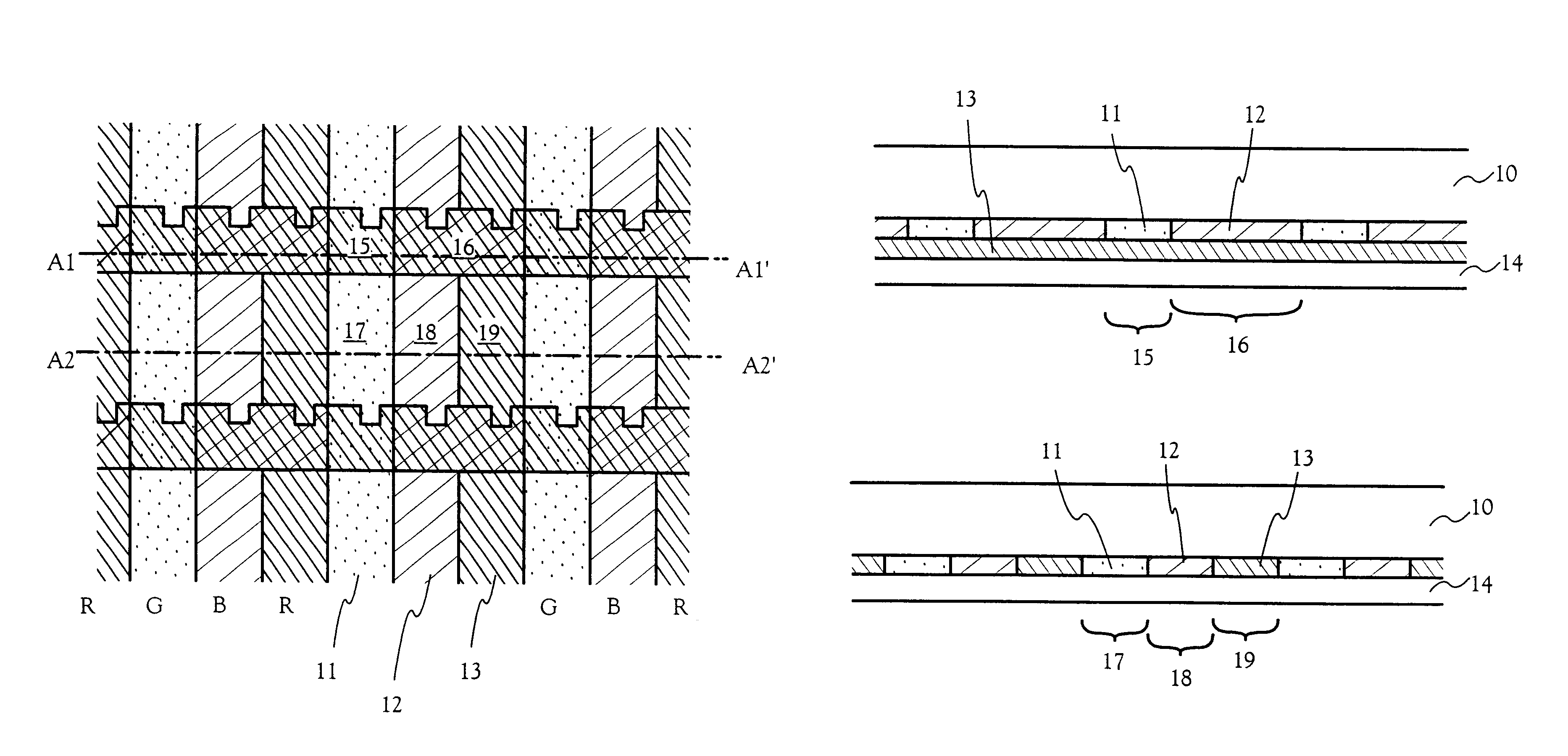
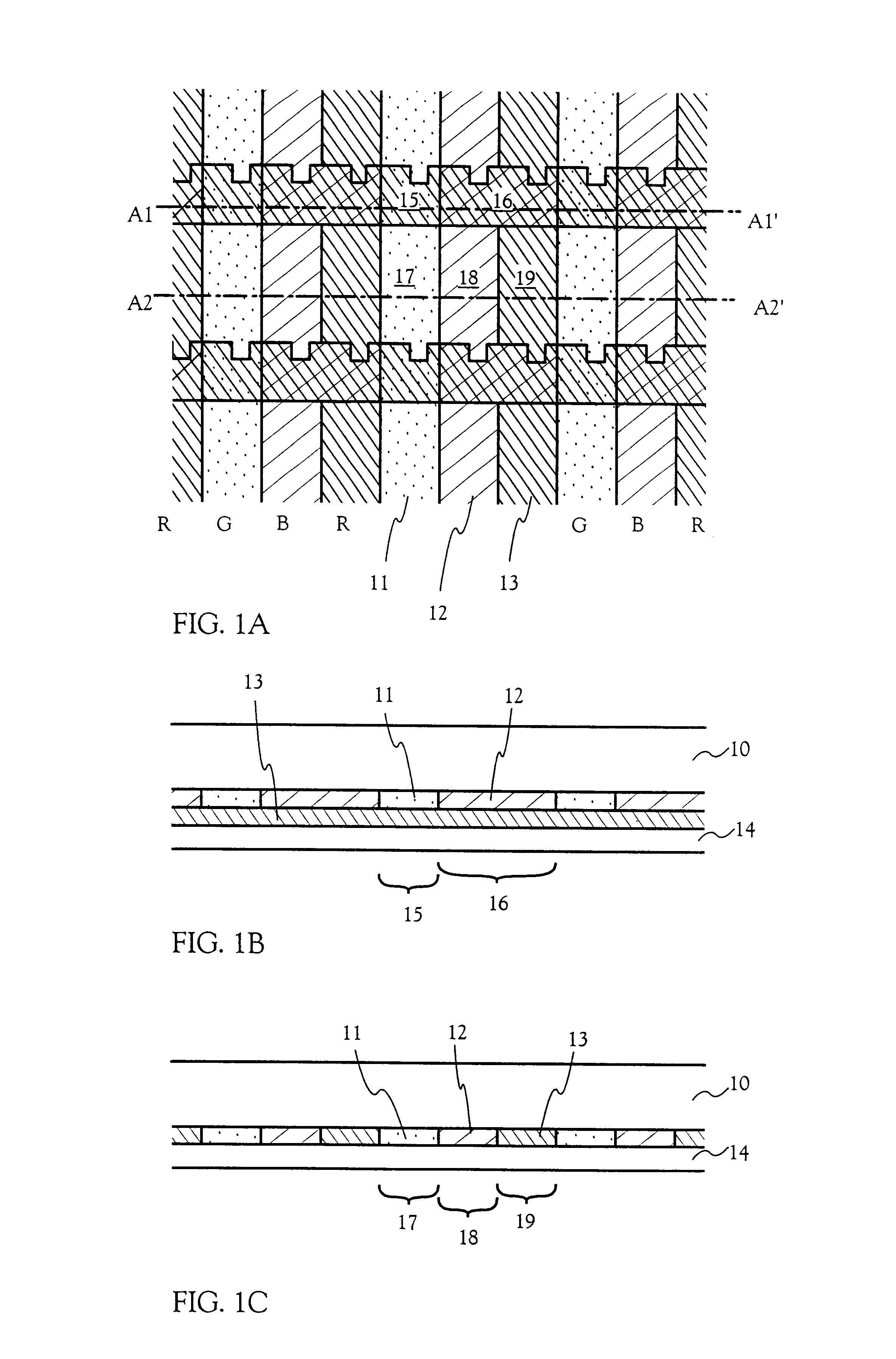
An embodiment of the present invention will be described hereinbelow with taking as an example a manufacturing of an opposing substrate which will be employed for an active matrix liquid crystal display device. FIGS. 1A-1C show an opposing substrate having colored layers which are formed according to the present invention.

First, as a substrate 10 having light translucent property, a glass substrate such as barium borosilicate glass or aluminum borosilicate, represented by such as Corning #7059 glass and #1737 glass is prepared. In addition to the above, a light translucent type substrate such as a quartz substrate and a plastic substrate may also be used.

Then, an organic photosensitive material (CGY-S705C: COLOR MOSAIC, manufactured by Fuji Film Olin Co.) is applied onto the opposing substrate 10, and the organic photosensitive material is patterned into stripe shape as shown in FIG. 1A by a photolithography method to form the green-colored layer (G) 11 at a predetermined position. ...

embodiment 2

In Embodiment 1, an example is shown in which the green-colored layer (G) 11, the blue-colored layer (B) 12, and the red-colored layer (R) 13 are formed in sequence. However, in this embodiment, a description will be made hereinbelow of an example of forming the respective colored layers in an order different from that in Embodiment 1. Note that, except the order of forming the respective colored layers, the other manufacturing steps are the same with that in Embodiment 1, thereby only different points will be described.

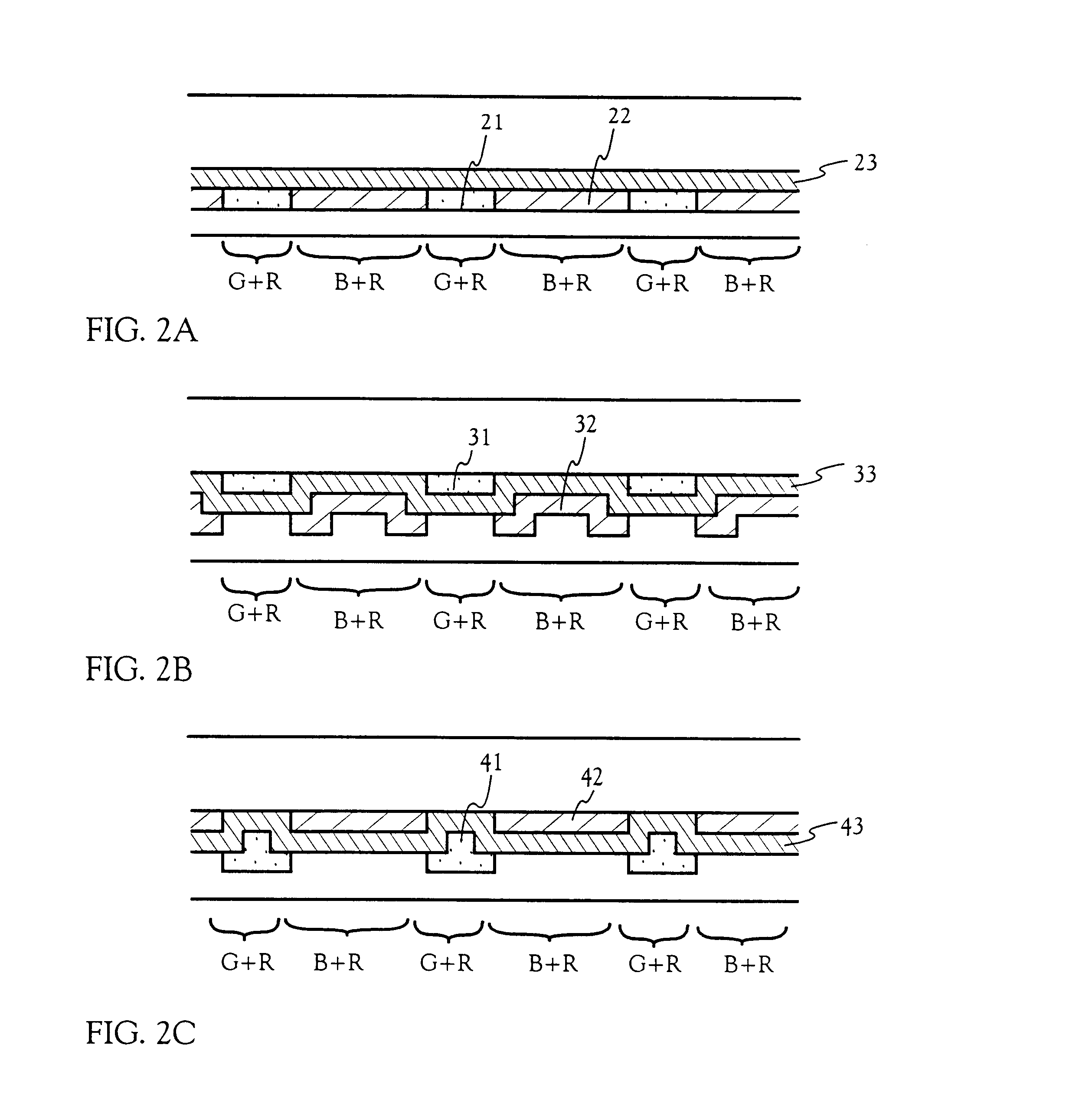
A structure shown in FIG. 2A may be taken as a first example. FIG. 2A shows an example in which a colored layer (R) 23 is first formed, and then, a colored layer (B) 22 and a colored layer (G) 21 are laminated thereon. Note that FIG. 2A corresponds to a sectional view taken along the dash line of A1-A1' of FIG. 1A.

Further, a structure shown in FIG. 2B may be employed as a second example. FIG. 2B is an example in which a colored layer (G) 31 is first formed, a colored...

embodiment 3

In this embodiment, a description will be made of a manufacturing method of a device substrate (also referred to as an active matrix substrate) which is stuck with an opposing substrate obtained in Embodiment 1 or Embodiment 2. Here, a method of simultaneously forming, on the same substrate, a pixel portion and TFTs (n-channel TFT and p-channel TFT) of a driver circuit formed in the periphery of the pixel portion, is described in detail.

First, in this embodiment, a substrate 100 is used, which is made from glass, such as barium borosilicate glass or aluminum borosilicate, represented by such as Corning #7059 glass and #1737. Note that, as the substrate 100, a quartz substrate, or a silicon substrate, a metal substrate, or a stainless substrate, on which an insulating film is formed, may be used as the replace. A plastic substrate having heat resistance to a process temperature of this embodiment may also be used.

Then, as shown in FIG. 5A, a base film 101 formed from an insulating fi...


PUM

PropertyMeasurementUnit
wavelengthaaaaaaaaaa
wave lengthaaaaaaaaaa
widthaaaaaaaaaa

Abstract

In a conventional liquid crystal display panel using a metallic film as a light shielding mask of a color filter, there arose a problem in that a parasitic capacitor with the other wiring is generated to often cause a delay in signal. Further, there arose a problem in that, if an organic film containing a black pigment is used as the light shielding film of the color filter, the manufacturing step thereof increases. In the present invention, lamination films of colored layers consisting of two layers (lamination film of a red-colored layer and a blue-colored layer, or lamination film of a red-colored layer and a green-colored layer) are formed on an opposing substrate as light shielding portions so as to overlap with TFTs on a device substrate without forming a light-shielding mask (black matrix).

Description

1. Field of the InventionThe present invention relates to a semiconductor device having a circuit constructed of a thin film transistor (hereinafter referred to as TFT), and to a method of manufacturing the same. For example, the present invention relates to an electro-optical device, which is represented by a liquid crystal display device, and to electronic equipment loaded with the electro-optical device (electric device) as a part.Note that, in this specification, the term semiconductor device indicates general devices that function by utilizing semiconductor characteristics, and that electro-optical devices, semiconductor devices, and semiconductor circuits are all included in the category of the semiconductor device.2. Description of the Related ArtIn recent year, a technique for constructing a thin film transistor (hereinafter referred to as TFT) using a semiconductor thin film (on the order of several to several hundreds nm in thickness) formed on the substrate having an insu...

Claims


Application Information

Patent Timeline
Patent Type & Authority Patents(United States)
IPC IPC(8): G02F1/13G02F1/1335
CPCG02F1/133514G02F1/133512
Inventor YAMAZAKI, SHUNPEIGOTO, YUUGO
Owner SEMICON ENERGY LAB CO LTD
Why Eureka
Try Eureka