

Plasma enhanced chemical vapor deposition of copolymer of parylene N and comonomers with various double bonds
- Summary
- Abstract
- Description
- Claims
- Application Information
AI Technical Summary
Problems solved by technology
Method used
Image

Examples
example 2
Tetraallyloxysilane
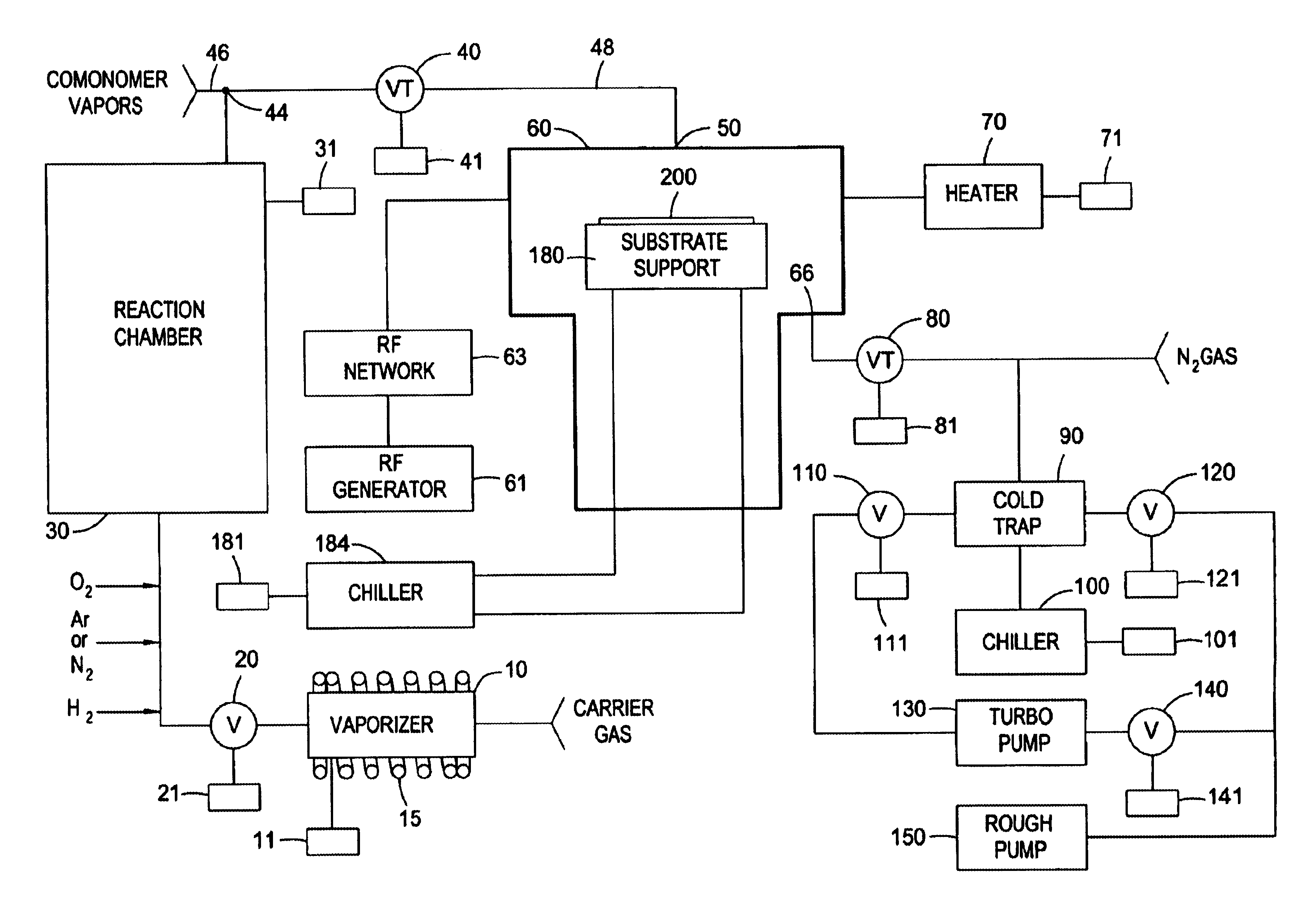
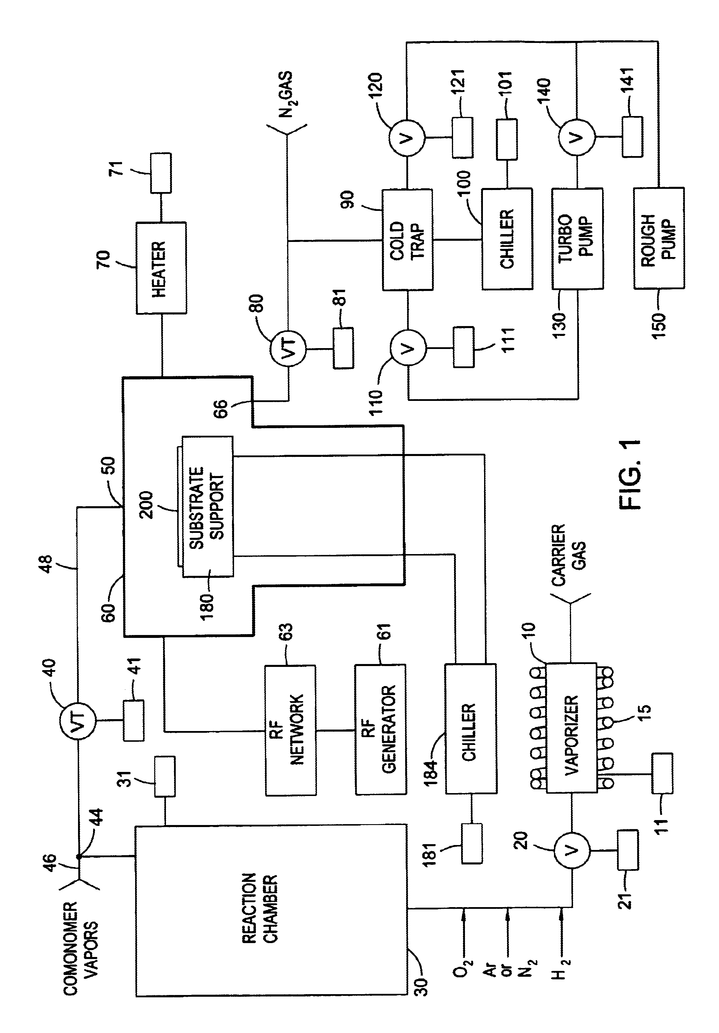
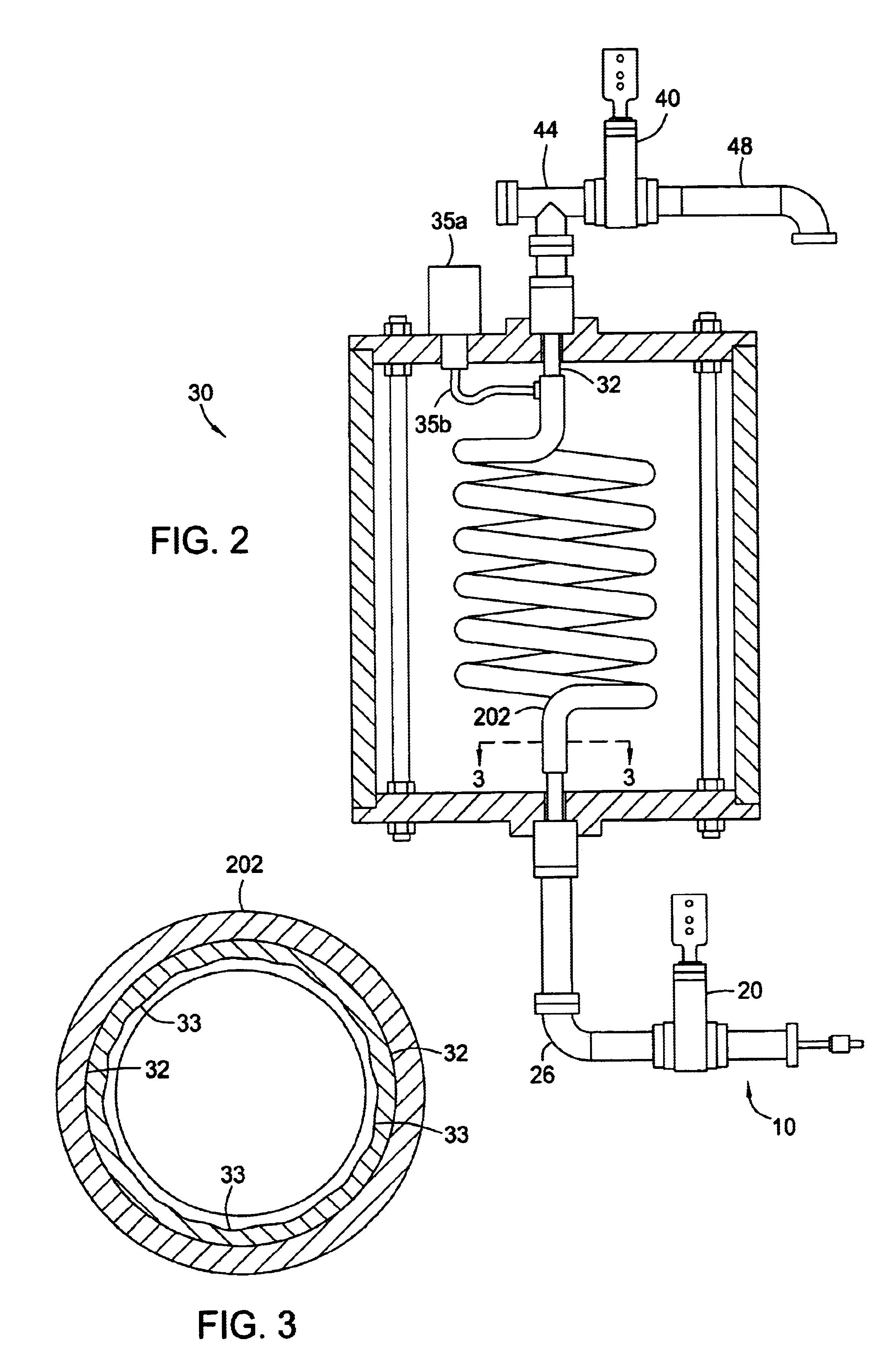
To further illustrate the process of the invention, an eight inch diameter silicon wafer was mounted on a fixed substrate support maintained at a temperature of about 25.degree. C. in a DLK deposition chamber, available from Applied Materials, Inc., of Santa Clara, Calif. The chamber was configured substantially as shown in FIGS. 1 to 8.
About 30 grams of particulate di-p-xylylene were loaded into the vaporizer 10 and the vaporizer was then heated to about 200.degree. C. The gate valve 20 separating the vaporizer 10 from the decomposition chamber 30 was then opened, and the vapors of dimer were allowed to flow through a mass flow controller into the reaction chamber 30 which was preheated to a temperature of about 850.degree. C. The exit gate valve 40 of the reaction chamber 30 was then opened and the vaporized reactive p-xylylene formed in the reaction chamber 30 then flowed from the reaction chamber through the heated conduit to the deposition chamber 60 at a rat...
example 3
Tetravinyltetramethylcyclotetrasiloxane
To further illustrate the process of the invention, an eight inch diameter silicon wafer was mounted on a fixed substrate support maintained at a temperature of about 0.degree. C. in a DLK deposition chamber as configured and described in Example 1. About 30 grams of particulate di-p-xylylene were loaded into the vaporizer 10 and the vaporizer was then heated to about 200.degree. C. The gate valve 20 separating the vaporizer 10 from the reaction chamber 30 was then opened, and the vapors of dimer were allowed to flow through a mass flow controller into the reaction chamber 30 which was preheated to a temperature of about 850.degree. C. The exit gate valve 40 of the reaction chamber 30 was then opened and the vaporized reactive p-xylylene formed in the reaction chamber 30 then flowed from the reaction chamber through the heated conduit to the deposition chamber 60 at a rate of about 10 sccm. The lid of the deposition chamber 60 was maintained at...
example 4
Trivinylmethylsilane Copolymer
To further illustrate the process of the invention, an eight inch diameter silicon wafer is mounted on a fixed substrate support maintained at a temperature of about 25.degree. C. in a DLK deposition chamber, available from Applied Materials, Inc., of Santa Clara, Calif. The chamber was configured substantially as shown in FIGS. 1 through 8. P-xylylene was provided by sublimation of di-p-xylylene and decomposition in a thermal reaction chamber 30 which is preheated to a temperature of about 650.degree. C. The exit gate valve 40 of reaction chamber 30 is then opened and the vaporized reactive p-xylylene formed in reactor 30 then flows to the deposition chamber 60 at a rate of about 40 sccm. The lid of the deposition chamber 60 is maintained at a temperature of about 150 to about 200.degree. C., and the walls of the chamber 60 are maintained at about 70.degree. C.
Trivinylmethylsilane is introduced into the chamber 60 at a rate of 10 sccm. About 50 sccm of...
PUM
| Property | Measurement | Unit |
|---|---|---|
| Percent by mass | aaaaa | aaaaa |
| Power | aaaaa | aaaaa |
| Power | aaaaa | aaaaa |
Abstract
Description
Claims
Application Information