Chip interconnect wiring structure with low dielectric constant insulator and methods for fabricating the same

a technology of low dielectric constant and wiring structure, which is applied in the direction of electrical equipment, semiconductor devices, semiconductor/solid-state device details, etc., can solve the problems of corrosion and adhesion loss, the physico-chemical properties of many of these low k materials are not optimum for the cmp process, and the practical difficulties of integrating low k dielectric materials in such a wiring structur

Inactive Publication Date: 2001-02-06
GLOBALFOUNDRIES INC
View PDF1 Cites 362 Cited by
  • Summary
  • Abstract
  • Description
  • Claims
  • Application Information

AI Technical Summary

Problems solved by technology

There are several practical difficulties in integrating the low K dielectric materials in such a wiring structure.
First, the physico-chemical properties of many of these low K materials are not optimum for the CMP process.
Fluorinated oxide dielectrics are suspected to react with or be prone to wiring methodologies leading to corrosion and adhesion loss.
Second, most of the low K polymers degrade under thermal excursions to temperature at or above 400.degree. C.
Hence, they are not suitable for the device interconnection application because they cannot withstand the device damage anneal alluded to above.
This severely restricts the choice of dielectric which can be used for this purpose.
Last, the porous inorganic dielectrics such as aerogels are mechanically weak and friable and are unlikely to withstand the multilayer build process of repeated metal deposition and CMP described above.
This can degrade the insulator's dielectric constant and leakage performance and in some cases, facilitate the migration of copper to the device levels during the service life of the chips, leading to device failure.
This is particularly severe for narrow lines typical of advanced chips, where the barrier thickness becomes a significant fraction of the line width itself.
Many of the low K dielectrics are also not compatible with Al--Cu interconnect processing because 400.degree. C. to 450.degree. C. substrate temperatures during deposition and/or post deposition anneals are still required to achieve reliable microstructure and properties of the Al--Cu lines, and repeated excursions to such temperatures (in addition to the final device damage anneal) tend to lead to degradation of many of the low K polymeric insulators, as mentioned earlier.
This method suffers from several limitations.
This makes it difficult to ensure definitively what the exact nature of the dielectric medium would be around any given line in an interconnect design.
This makes the task of predicting and acc...

Method used


Image

  • Chip interconnect wiring structure with low dielectric constant insulator and methods for fabricating the same
  • Chip interconnect wiring structure with low dielectric constant insulator and methods for fabricating the same
  • Chip interconnect wiring structure with low dielectric constant insulator and methods for fabricating the same

Examples


first embodiment

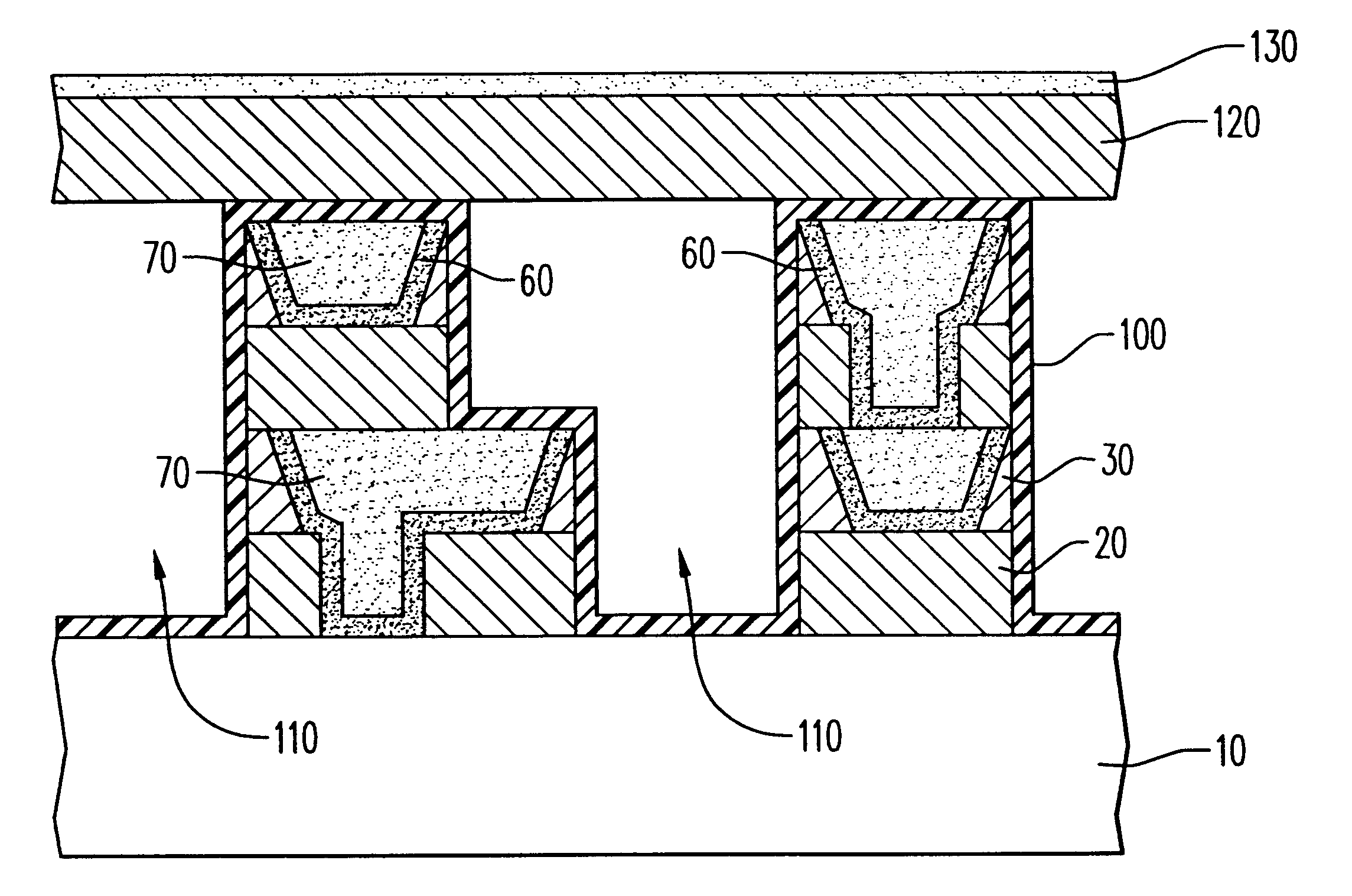
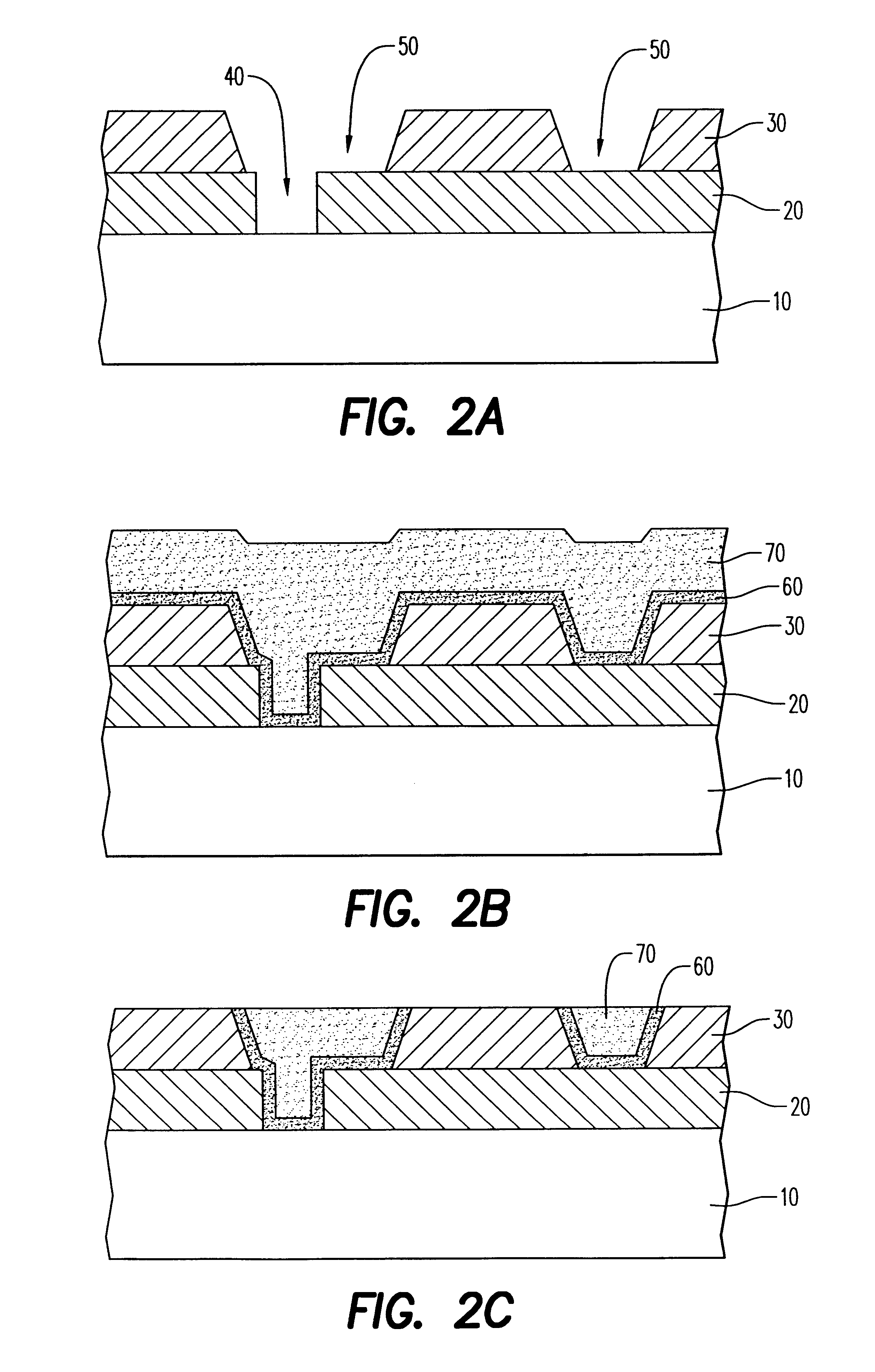
The etch back approach proposed in the present invention was demonstrated by an experiment using a test wiring structure. This structure comprised an oxidized silicon substrate with a first wiring layer of copper, a second via level of copper and a third wiring level of copper connected to the first level at selected locations by means of said second copper vias. The insulator separating the different levels was Dupont Pyralin 2611 polyimide about 1.2 .mu.m thick. The line widths of the metal features ranged in size from 1 to 4 .mu.m, with spacings ranging from 0.65 to 3.75 .mu.m, and the metal thickness was about 1.2 .mu.m. There was a 100 nm layer of SiO.sub.2 deposited between the layers and on the third polyimide layer to act as CMP and RIE stop layer since these parts were fabricated by the damascene process described above in the

This structure was subjected to RIE to remove the dielectric layers from between the metal features. Typical RIE conditions employed for the polyimide...

example 2

An oxidized silicon wafer with two wiring levels interconnected at selected location by a via level was the starting point for this experiment. The structure consisted of Al--Cu alloy wiring and via studs and Ti-based or Ta-based adhesion and cap layers approximately 100 nm thick. The dielectric used was PECVD SiO.sub.2 and the build process used to make these substrates was one where the metal lines were fabricated by subtractive patterning followed by overcoating with the oxide dielectric material which was deposited by PECVD process. The features were typically 0.5 to 5 .mu.m in width and spacings in different locations of the wafer.

The wafer was subjected to RIE in CF.sub.4 or CHF.sub.3 / O.sub.2 plasma which was 80 to 95% fluorocarbon containing and in the pressure range of 10 to 30 mTorr, at an rf power density of 0.25 to 1 Watt / cm.sup.2. FIG. 6 is an SEM photograph of the structure after the completion of the etching process. It is evident that the oxide dielectric has been fu...

example 3

In an effort to demonstrate the etch back approach followed by conformal coating of a thin passivation dielectric proposed in the present invention, an experiment was performed using a test wiring structure. The structure was identical to the one described in Example 1 comprising wiring trace-via-wiring trace levels with polyimide dielectric between the metal features.

This structure was subjected to RIE to remove the dielectric layers from between the metal features. Typical RIE conditions employed for the polyimide removal were 10 to 30 mTorr of a CF.sub.4 / O.sub.2 gas mixture with 80 to 95% oxygen, at an rf power density of 0.25 to 1 Watt / cm.sup.2. The oxide RIE was carried out in a pure CF.sub.4 gas under similar conditions.

At this point, the wafer was loaded on a grounded substrate holder of a plasma enhanced chemical vapor deposition (PECVD) chamber, and coated with a 20 nm of silicon nitride using a process gas containing 2% silane in helium (30 sccm flow rate) and nitrogen (2...


PUM


Abstract

A method to achieve a very low effective dielectric constant in high performance back end of the line chip interconnect wiring and the resulting multilayer structure are disclosed. The process involves fabricating the multilayer interconnect wiring structure by methods and materials currently known in the state of the art of semiconductor processing; removing the intralevel dielectric between the adjacent metal features by a suitable etching process; applying a thin passivation coating over the exposed etched structure; annealing the etched structure to remove plasma damage; laminating an insulating cover layer to the top surface of the passivated metal features; optionally depositing an insulating environmental barrier layer on top of the cover layer; etching vias in the environmental barrier layer, cover layer and the thin passivation layer for terminal pad contacts; and completing the device by fabricating terminal input/output pads. The method obviates issues such as processability and thermal stability associated with low dielectric constant materials by avoiding their use. Since air, which has the lowest dielectric constant, is used as the intralevel dielectric the structure created by this method would possess a very low capacitance and hence fast propagation speeds. Such structure is ideally suitable for high density interconnects required in high performance microelectronic device chips.

Description

This invention pertains to the field of microelectronic chip fabrication for logic, memory, communication and microcontroller applications.BACKGROUND OF INVENTIONThe operating speeds of silicon integrated circuits are increasing at phenomenal rates to meet aggressive performance demands in computing, communication and microcontroller applications. This in turn necessitates that the signal propagation delays in the wiring that is used to interconnect the circuits on a chip be reduced so that the performance is not limited or hampered unduly by interconnect delays. Interconnect delays in chips are due to the RC time constants wherein R is the resistance of the on chip wiring and C is the effective capacitance between the signal lines and the surrounding conductors in the multilayer interconnection stack. The resistance of the wiring can be reduced by using a material with a lower specific resistivity than the currently used Al-rich Al--Cu alloys. Copper, which has half the specific re...

Claims


Application Information

Patent Timeline
IPC IPC(8): H01L21/70H01L21/768H01L23/522H01L23/52H01L23/532
CPCH01L21/7682H01L23/5222H01L23/53223H01L23/53228H01L23/53238H01L23/5329H01L2924/0002H01L2924/00
Inventor BUCHWALTER, LEENA P.CALLEGARI, ALESSANDRO CESARECOHEN, STEPHAN ALANGRAHAM, TERESITA ORDONEZHUMMEL, JOHN P.JAHNES, CHRISTOPHER V.PURUSHOTHAMAN, SAMPATHSAENGER, KATHERINE LYNNSHAW, JANE MARGARET
Owner GLOBALFOUNDRIES INC
Why Eureka
Try Eureka